
Polar Light, Finetech Partner on Micro-LED Tech
Semiconductor equipment solutions provider Finetech and microLED developer Polar Light have partnered to advance microLED technologies for next generation AR, head-up, and head-mounted display applications. The collaboration aims to advance novel gallium nitride (GaN) pyramidal microLEDs developed by Polar Light that feature microLEDs directly bonded to indium pads on a silicon chip.
The fabrication method, in which LEDs are built from the bottom up, avoids the surface damage seen in traditional top-down methods, resulting in better optical performance. The pyramidal shape of these LEDs enables smaller size, higher brightness, and greater emission efficiency, the companies said.
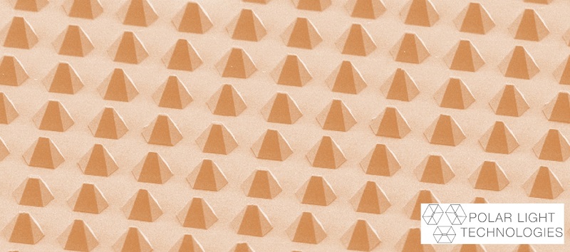
Polar Light has developed a bottom-up fabrication process for pyramidal microLEDs that enables smaller size, higher brightness, and better emission efficiency. The process utilizes a cold compression bonding method developed with Finetech. Courtesy of Polar Light Technologies.
Polar Light's collaboration with Finetech focuses on connecting these pyramidal microLEDs to silicon substrates. Because of differences in how ilicon carbide and silicon expand with heat, no heat can be used during the bonding process. Finetech and Polar Light Technologies developed a cold compression bonding method for aligning and bonding microLED arrays using an automated FINEPLACER femto 2 sub-micron die bonder. The companies reported an 85% success rate in early trials, which they said shows its potential for large-scale manufacturing.
Polar Light’s approach to making display front panels involves a bottom-up fabrication method using atomic layer regrowth. The company grows the GaN microLEDs on a silicon carbide substrate in a method that produces microLEDs as small as 300 nm without the damage that traditional top-down fabrication methods may cause. As a result, the devices have nearly perfect surfaces, which is crucial for optical properties.
The microLED displays developed through this process can fit the resolution of a full TV screen into an area smaller than 5 mm², with about 1000 x 1000 connection points spaced just 5 µm apart. Polar Light’s design also significantly reduces energy use, making these microLEDs efficient for next-generation micro displays.
Compared to regular LEDs, the companies said, the pyramidal microLEDs improve AR system efficiency by 50 to 200 times as a result of better internal and external quantum efficiencies and enhanced light utilization. Further, by minimizing internal electric field interference and optimizing the interaction between charge carriers in the quantum wells, the developed microLEDs produce more light with sharper, more narrow emission. This quality makes the microLEDs viable for applications like AR where precise light control is important.
/Buyers_Guide/Polar_Light_Technologies/c33963
/Buyers_Guide/FINETECH_GmbH_Co_KG/c4948