Plasma Deposition Yields Thin Films of Optically Active Dyes
Daniel S. Burgess
Scientists in Europe have reported the development of a single-step, room-temperature plasma-enhanced chemical vapor deposition process that yields polymeric thin films incorporating isolated rhodamine molecules. They note that the method is compatible with lithographic fabrication processes and propose that the films may find application as optical filters, including for use in LCDs.

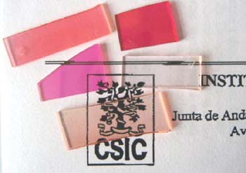
Created by plasma-assisted chemical vapor deposition, the thin films feature molecules of rhodamine 6G in a host of silica. Courtesy of Ángel Barranco.
Ángel Barranco, an investigator at the Spanish National Research Council’s Instituto de Ciencia de Materiales de Sevilla, further suggested that the process may be used with a variety of dyes suitable for integrated photonic systems for use in trace gas sensing, in the monitoring of temperature and of UV irradiation, and in wavelength shifters. He collaborated on the work with Pierangelo Gröning of the Nanotech@surfaces Laboratory at Eidgenössische Materialprüfungs- und Forschungs-Anstalt in Thun, Switzerland, and is the coordinator of Phodye, a multidisciplinary project funded by the European Union that is investigating dye-based photonic systems for sensing applications.
“We think the method opens a lot of real possibilities for the fabrication of photonic devices integrating optically active thin films,” Barranco said.

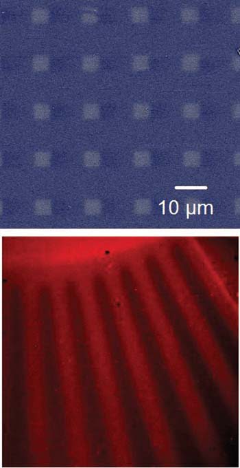
Scanning electron microscope (top) and fluorescence (bottom) images reveal, respectively, the structure of a lithographically patterned film and its emission.
In a demonstration of the approach, the researchers sublimated the fluorescent dye rhodamine 6G in the downstream region of an electron cyclotron resonance microwave plasma of argon and trimethylsilane. They found that the process yields films comprising nanocomposites of silica and nonaggregated dye molecules, which prevents fluorescence quenching.
Using atomic force microscopy, the scientists established that the films are homogeneous and are free of surface defects such as cracks, with a measured surface roughness of 0.6 nm rms for a 90-nm-thick sample. Absorption and fluorescence emission and excitation spectra indicated that the films feature intact rhodamine molecules suspended in a cross-linked matrix formed by fragments of the dye and trimethylsilane.
Barranco said that the plasma deposition process promises to be an effective alternative to sol-gel synthesis and other chemical routes as a result of its simplicity, speed, flexibility and compatibility with silicon manufacturing techniques. Classical chemical synthesis routes, he explained, may involve several steps of drying, curing and heating, sometimes requiring several days, and they do not offer the precise control of chemical vapor deposition over a film’s thickness and planarity on the nanometer scale.
He said that the investigators are working with several families of optically active dyes in hopes of producing films that incorporate multiple dyes with complementary characteristics in alternative host materials, including TiO2. They also plan to publish the results of an initial investigation into the use of the films for sensing applications.
Langmuir, Aug. 1, 2006, pp. 6719-6722.
Published: September 2006