Scott Jordan, PI (Physik Instrumente)
Microscopy is a broad field – and it is getting broader every week, as novel imaging techniques are brought to bear to illuminate the nanoscale world. These techniques are enabled and assisted by the application of piezoelectric positioning mechanisms, including newly developed types based on diverse physical applications of piezoelectric ceramics.
The intersection of nanopositioning and microscopy is expanding and deepening rapidly. The evolution of disciplines as diverse as single-molecule biophysics, superresolution microscopy and automated microassay scanning share several common themes: a prerogative for higher throughput, rapidly diminishing resolution tolerances, more dynamic (on the fly) techniques, and burgeoning opportunities for commercialization. These combine to increase the need for piezo-based positioning systems to be added or integrated into microscopic setups.
Recently developed mechanisms of significant relevance to microscopic applications present substantial new opportunities for advancement. Some are enablers for new applications; others address previous constraints.
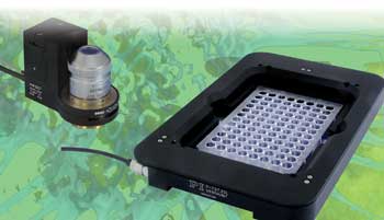
Nanopositioning can allow microscopists to do things they never could before. The PIFOC piezo lens positioner and Piezo-Z Stage allow for precise Z-axis positioning. Courtesy of PI (Physik Instrumente) LP.
If there is one thing that is predictable about the future of this field, it is that application needs and the capabilities of piezoelectric actuation will continue to chase each other, to the benefit of science and society.
Focusing applications
Piezoelectric actuators have traditionally been layered structures of lead zirconate titanate (PZT) ceramic interleaved with electrodes. This ceramic is ferroelectric, and application of a varying voltage produces a nearly proportional change in dimension. The dimensional change can be controlled to exquisite levels, which is why PZT actuation has been the foundation of atomic force microscopes and other applications requiring nanoscale-controlled motions. But PZT actuation also is very quick, so throughput has been another reason for adoption.
In microscopy, a common application is Z-stack data acquisition, in which either the sample or the focusing lens is rapidly stepped or scanned along the optical axis. PZT mechanisms are the choice for this because of their combination of speed and precision. Integration of a frictionless lever amplification element allows design of compact and cost-effective mechanisms with many hundreds of microns of travel. Incorporation of a position sensor such as a strain gauge or a capacitive sensor allows the PZT actuation to be made highly linear and repeatable, and users thereby can acquire position information synchronously with the optical data without stopping, ensuring a reliable and highly deterministic position-domain abscissa for their data.
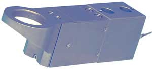
The new 1-mm PIFOC focusing drive is shown with NEXACT piezo motors. Courtesy of PI (Physik Instrumente) LP.
In these applications, a recent trend has been toward longer and longer scan travels – even beyond the several-hundred-micron travels of which conventional lever-amplified PZT mechanisms are capable. Long travel is especially important for microscopy applications with large penetration depth, such as two-photon microscopy. This has necessitated development of novel mechanisms that use revolutionary modalities of piezo actuation.
For example, in a class of walking-style actuators, the piezo ceramic is configured in a manner that confers longitudinal force on a ceramic actuation rod of arbitrary length. The ceramic elements can be actuated down into the subnanometer realm for small distances, or they may be phased to alternately push and retract, allowing unlimited travel actuation with high axial stiffness and holding force – ideal for focusing mechanisms where stiffness is desirable for stability reasons and to accommodate heavy, high-numerical-aperture objectives.
Similarly, piezo actuation’s high speed and resolution make it the ideal technology for especially responsive autofocus implementations in microscopy. In particular, a unique laser autofocus sensor can be seamlessly combined with piezo nanopositioning controls to provide continuous real-time focusing of moving or evolving samples in surface science and biotechnology applications.
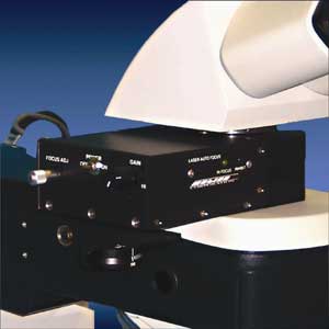
A laser autofocus sensor such as this model from Motion X Corp. of Goleta, Calif., can be seamlessly combined with piezo nanopositioning controls to provide continuous real-time focusing of moving samples. Courtesy of Motion X Corp.
This approach offers many benefits over previous, probe-based platform stabilization methods that merely compensate for structural deflections of the microscope platform or other gross elements. Responsiveness is millisecond-scale, and all structural and optical contributors to defocusing are automatically compensated, even during motion.
Scanning applications
Transverse motion of the sample across the image field is another near-universal requirement in microscopy applications. Depending upon the application, the required motions can be coarse – over the many millimeters of a slide or well plate – or they can be fine, with nanoscale precision over just a few dozen microns of range. They can be point-to-point or linear scans of constant velocity – or even with specific position-vs.-time waveforms, as in the case of calibrating optical tweezers. Very often, there is a requirement for both coarse and fine actuation, so that a region of interest can be brought into the field of view and then scanned at high resolution.
Scanning can be accomplished by optical means such as using beam-steering mirrors or acousto-optic deflectors, but moving the sample using a piezo flexure stage offers benefits for applications requiring the highest resolution and flattest scanning and positioning. Piezo flexure stages can provide up to 2 mm of scanning range, but more typically a less costly piezo stage in the ~50- to 200-µm range is stacked on top of a coarse positioning stage.
Such coarse/fine applications have seen noteworthy benefits from piezo-based technical developments in recent months. In particular, coarse-positioning mechanisms using a third type of piezoelectric actuation – besides the layered-stack actuators used in nanoscale positioning and the walking-type described for long-travel focusing mechanisms – employ matchbook-size slabs of piezoelectric ceramic that are stimulated at their physical resonant frequency, typically in the ultrasonic range above 100 kHz.
This stimulation causes a rhythmic fluttering of the slab, and a friction tip placed at the resonance’s antinode performs a quasi-elliptical nanoscale motion. When preloaded against a driven element, this confers a motive force. The stimulus-to-velocity profile of this actuation is similar to that of familiar DC servomotors, but the prominent deadband, or neutral zone, in the actuation profile means that the device holds the driven element with nanoscale stabilities when quiescent. In addition, lubricant flow mechanisms that cause long-term drift and settling behaviors in conventional, screw-driven coarse-positioner mechanisms are eliminated.
The resulting long-term nanoscale stability and innate position-hold force of these mechanisms have improved resolution and repeatability in a variety of leading-edge applications. They also promise significant benefits in stitching applications, where high-resolution imaging is performed in small areas that are subsequently patched together in software.
Ultrasonic piezomotors are therefore especially attractive for transverse sample positioning in coarse/fine microscopy applications. They provide the long travel over many millimeters necessary for quickly accessing the full span of a microscope slide or well plate, and they offer an inherently stiff and stable platform at rest.
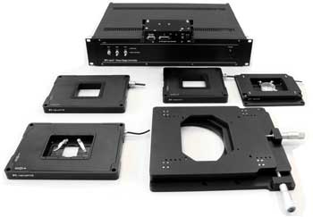
The PInano microscope stage family enables a wide range of scientific applications. Courtesy of PI (Physik Instrumente) LP.
In fact, data published in a recent peer-reviewed paper in a compendium of the 2009 Aspen Conference on Single Molecule Biophysics documents nanoscale stabilities over many minutes for a combined coarse/fine stack based on an ultrasonic piezomotor coarse stage and a PZT-stack-based multiaxis nanopositioner – performance shown to be roughly an order of magnitude more stable than a high-quality screw-driven manual positioning stage [“Design considerations for micro- and nanopositioning: leveraging the latest for biophysical applications,” by S.C. Jordan and P.C. Anthony (August 2009), Current Pharmaceutical Biotechnology, Vol. 10, pp. 515-521. Full article at http://www. bentham.org/cpb/sample/cpb10-5/0008G% 5B1%5D.pdf].
Sensors
Several types of position sensors are used in closed-loop nanopositioning mechanisms. The highest-resolution, -bandwidth, -accuracy and -stability sensor is the two-plate capacitive, in which one highly polished and complexly configured metallic plate is mounted on the moving element of a stage, with a corresponding plate on the fixed structure of the stage. As the stage moves, the actual position of the workpiece is measured in real time.
These sensors may be arrayed around the workpiece to monitor its position in multiple degrees of freedom, facilitating parallel-kinematic configurations in which a single workpiece is actuated simultaneously in several directions. This increases system bandwidths and improves trajectory performance over less costly stacked multiaxis designs.
For applications where the resolution, accuracy, bandwidth and stability of capacitive sensors are not needed, various strain gauges have been used. Thin-film strain gauge sensors, for example, mount on the piezo stack and measure its expansion and contraction, allowing the servocontroller to linearize its actuation and eliminate hysteresis. These sensors span a significant area, so they are comparatively insensitive to local effects.
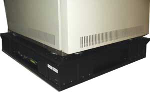
Shown is an active isolation platform for instrumentation such as scanning electron microscopes and life-sciences microscopes. Courtesy of Technical Manufacturing Corp., Peabody, Mass.
By comparison, silicon piezoresistive sensors are very small, ideal for incorporation into a flexure element of a stage’s structure. These are the foundation for a new wave of high-quality but cost-effective US-made family of nanopositioners targeted at research and commercial microscopy applications.
Vibration isolation
As resolutions increase and microscopy techniques emerge from the lab and become incorporated into commercial tools and processes, protection from ambient vibrations has become critical. Here, too, piezoelectric technology assists in advancing the field. Active vibration control technology has long been a mainstay of semiconductor microlithographic manufacturing and is fundamental to achieving today’s rapidly diminishing integrated circuit linewidths, which routinely better 32 nm today. The leading active vibration control platforms depend on piezoelectric speed, resolution and reliability to routinely enable such performance on the production floor,1 and, recently, these platforms have found their way into the most advanced microscopy applications as well.
Meet the author
Scott Jordan, a physicist by training with an MBA in new venture management and finance, is director of nanoautomation technologies for PI (Physik Instrumente) LP in Auburn, Mass. Information: Stefan Vorndran, VP of marketing; email: [email protected].
Reference
1. S. Jordan and W. Wigglesworth (2010). Vibration and throughput: the yield killers. Eurasia Semicon. Issue 11, pp. 24-28. http://publishing.yudu.com/A1noip/EASemicon112010/resources/24.htm.