JIM BOVATSEK, MKS/SPECTRA-PHYSICS
With legislative and
environmental considerations converging into powerful tailwinds, the e-mobility sector is a blossoming innovation area in all reaches of its value chain. Today,
electric vehicle (EV) battery packs are scaling to higher voltages, achieving
levels as high as 800 V in some cases.
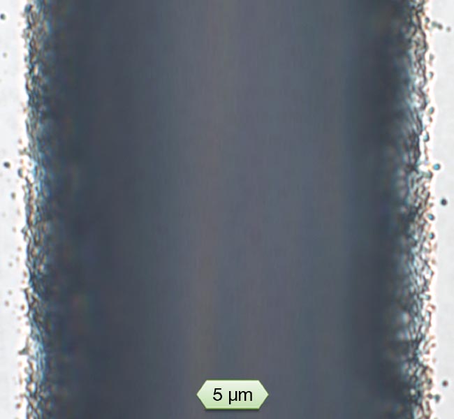
A close-up microscopic view shows that UV picosecond pulses in burst mode generate excellent edge quality, devoid of large chipping. Such a result is elusive for traditional mechanical saw processing. Courtesy of MKS/Spectra-Physics.
This increase provides benefits including greater horsepower, improved efficiency, increased range, and faster charging times. Within the vehicle, power electronics devices convert high direct current voltage into the forms that various
systems require. Traction motors, for example, require a three-phase alternating current. On-board chargers, meanwhile, dynamically adjust the current and voltage.
Despite its broad utility in many reaches of consumer and power electronics, silicon inflicts a bottleneck on this upscaling. Power electronics based on traditional silicon integrated circuits (ICs) do not work well with high voltages,
temperatures, and switching frequencies.
As a result, manufacturers must turn to other semiconductor materials to realize the full advantage of high voltage battery packs in EVs.
The single most promising alternative semiconductor is silicon carbide (SiC). This material offers characteristics that are almost ideal for EV power electronics, and, as a result, SiC holds the key to improving the performance and range of EVs as their popularity grows.
However, fabricating SiC devices is not without its own challenges. In a field in which established processes and protocols dominate, the mechanical, chemical, electronic, and optical characteristics of SiC differ significantly from silicon. The hardness of SiC, for example — the material is one of the hardest known materials, on par with diamond — makes wafer dicing using conventional mechanical methods, such as sawing, problematic. SiC is also a brittle material and chips easily when it is saw-cut. Additionally, SiC rapidly wears saw blades, including
those fabricated with hard diamond, necessitating the frequent replacement of this costly consumable. Saw cutting itself is a relatively slow process and generates heat that is apt to negatively affect the material properties.
The combination of these obstacles creates a roadblock for EV manufacturers, since many proven IC fabrication processes do not work the same way, or work at all, with SiC.
Singulation, or wafer dicing, is a prime example; mechanical sawing, which is the dominant method for singulating silicon wafers, does not effectively translate to SiC. Though laser singulation is promising, substituting the materials translates to — at minimum — a changed set of parameters for the process. End users must also identify the optimal sources for SiC singulation compared to the conventional approach using silicon.
Picosecond laser ablation
SiC device fabrication is performed the same way as in traditional silicon
microelectronics: Large numbers of
individual ICs are created on a single wafer and then singulated into individual chips. These chips are then prepared for packaging.
The reduction or full elimination of edge chipping, versus mechanical sawing, is imperative when dicing brittle SiC
wafers. Singulation should also cause minimal mechanical changes in the material. The minimization of kerf width should be prioritized, too, to limit the “street” size — the empty area between adjacent circuits — and thereby maximize the number of dies per wafer.
An engineer must balance these factors against cutting speed, yield, and other determinants that affect cost. The use of consumables such as coolants and cleaning fluids in the cutting process poses additional considerations.
Ultrashort-pulse lasers in the picosecond and femtosecond pulse width regime are established for high-precision cutting and ablation of many different materials, including hard, transparent, and/or brittle materials. Minimal bulk heating of the material and a negligible heat-affected zone (HAZ) are among the benefits of using ultrashort-pulse widths for processing. These sources also yield improved edge quality and less debris production compared with other classes of lasers.
The infrared output of most picosecond lasers can be frequency multiplied to deliver visible green or UV light, and the UV wavelength is often chosen for demanding applications. Sources operating in this band can typically achieve smaller focus spot sizes and an increased depth-of-focus, or Rayleigh range, at a given spot size.
These qualities make UV picosecond lasers a top choice for producing high
aspect ratio features and thinner kerf width cuts with more precise depth control. Also, the larger depth-of-focus makes these sources easier to implement in wide-field galvanometer scanning
systems. And the limited penetration of UV light further minimizes the HAZ.
Experimental setup
Still, achieving higher throughputs with short pulse widths and short wavelengths can be challenging in any setting. To ensure the repeatability of results in the context of SiC singulation, different system designs and parameters must be trialed. MKS/Spectra-Physics performed a series of cutting tests to evaluate the prospects for a UV picosecond pulse laser to deliver performance benefits, such as smaller focus spot sizes and increased depth of focus. These trials also sought to achieve physical advantages pertaining to ease of implementation and a decreased HAZ. Finally, beyond gauging the technical and economic viability of this process, these tests aimed to investigate how various pulse burst configurations might influence results.
In a first round of tests, samples of 340-µm-thick 4H-SiC wafers were
processed with a 50-W, 355-nm picosecond laser. The laser offers >60-µJ
maximum pulse energy and delivers
50 W of average power at repetition rates of 750 kHz to 1.25 MHz. It can be operated at a maximum of 10 MHz. Tests were performed at repetition rates between
200 and 400 kHz to ensure that all pulse output formats remained at similar levels of pulse energy and average power to enable a direct comparison of results.
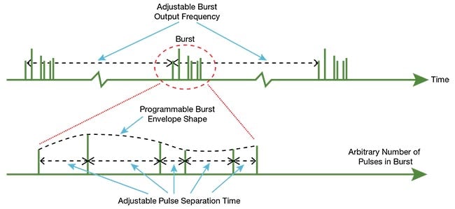
Figure 1. Both the temporal spacing and overall amplitude envelope of a pulse burst are controlled with precision. The system shown is an MKS/Spectra-Physics IceFyre UV 50 laser applying the TimeShift technology feature to achieve constant pulse energy and pulse width at any frequency at which the pulses are triggered. Courtesy of MKS/Spectra-Physics.
The picosecond laser was paired with a two-axis galvanometer scanner and a 330-mm focal length f-theta objective. The focus spot size at the work surface was ~30 µm (1/e2 diameter). The scanner was operated at speed ranges between
2 and 4 m/s, and multi-pass scanning was used for each scribe, delivering net
cutting speeds between 12.5 and 25 mm/s.
The laser used in these tests supported pulse bursts: The laser emitted a series
of closely spaced burst subpulses,
followed by a time gap before the next burst sequence. Although the laser-material interaction that occurs with pulse bursts remains an active field of investigative study, it has been well established in practice that pulse bursts can increase ablation rates and reduce surface roughness in many materials processing scenarios.
Discoloration around the scribe, which indicates a change in the surface or bulk material, shrinks and then disappears for higher pulse counts. The higher pulse counts also provided the best results at higher feed rates.
Moreover, the laser used in testing supported programmable pulse bursts. This means that the number of pulses in the burst, as well as the amplitude and the temporal spacing of each pulse in the burst, were controllable. Further, the timing jitter on the bursts was low enough to enable placement directly on the worksurface at levels of high precision, even at rapid scan speeds. These flexible pulsing capabilities enabled the exploration of a wide “process space” during testing.
Interpreting results
Figure 2 plots scribe depth values as a function of average laser power for various pulse burst configurations spanning a single pulse to a 12-pulse burst. For each test, the scribe was produced with a total of 80 passes over the same location on the material. Close control over the placement of each individual pulse burst on the work surface — the total pulse overlap — was maintained. In this case, the effective spatial overlap of the pulses was ~84%. These results demonstrate that the use of pulse bursts significantly improves the ablation rate. This outcome was expected and is consistent with the use of picosecond laser burst processing in other materials. Similarly, the ablation threshold decreased (essentially logarithmically) with the number of pulses contained in each burst. This demonstrates the “incubation” phenomenon that generally occurs in many materials with multipulse irradiation.
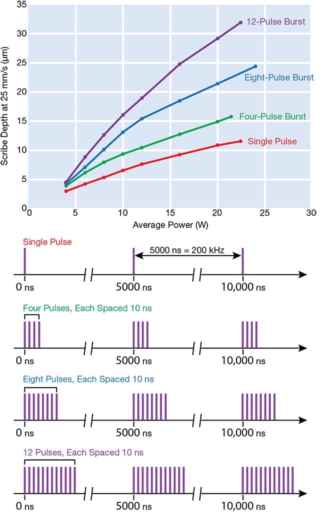
Figure 2. The depictions show scribe depth(s) for four passes at 25 mm/s as a function of power for single pulses (single pulse) and various burst configurations (four, eight, and 12 pulses). The data shows how pulse bursts improve ablation rates. Courtesy of MKS/Spectra-Physics.
Both 3D and 2D surface topography tools were used to precisely measure scribe depth and edge quality. An image obtained with a scanning white light interferometer shows a scribe in further detail (Figure 3). With a surface that is smooth and free of chips, the picosecond UV laser delivered another expected result: high-quality cuts.
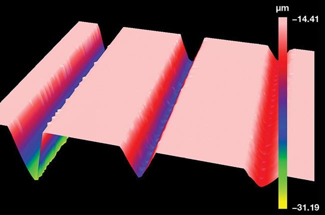
Figure 3. Scribes obtained with a scanning white light interferometer verify that the picosecond UV laser delivers clean, debris-free cuts. Courtesy of MKS/Spectra-Physics.
Further qualitative assessment of the scribes can be derived from Figure 4. The individual images show a series of 25-µm depth grooves produced with 1-, 4-, 8-, and 12-pulse bursts, successively. The average power was adjusted as needed to obtain the best results for each case. The four images in the top row are focused on the top surface of the wafer. The four images in the bottom row are focused on the floor of the scribe. Figure 4e-h shows a clear comparison and progression of cut quality as a function of the number of pulses in each burst.
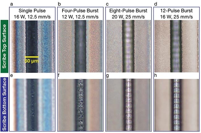
Figure 4. Close-up images of the tops (a-d) and floors (e-h) of 25-µm deep grooves. The grooves, at various values, show steady improvement in cut quality as the
number of pulses in the burst increases. Courtesy of MKS/Spectra-Physics.
Discoloration around the scribe, which indicates a change in the surface or bulk material, shrinks and then disappears for higher pulse counts. The higher pulse counts also provided the best results
at higher feed rates. This indicates that
the process can simultaneously deliver
adequate throughput and favorable
quality.
Figure 5 isolates higher magnification views of the floors of a series of scribes, all made under the same laser operating conditions of 16 W of average power and a net processing speed of 25 mm/s. The scribe depth for each condition is shown as a range from 8 to 25 µm at differing pulse burst values. This higher resolution view highlights the improvement in smoothness with increasing pulse count. For a constant average power and overall processing speed, tailoring the pulse output delivered a threefold increase in scribe depth.
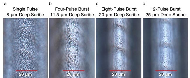
Figure 5. The extremely good edge/surface quality that can be achieved with picosecond UV laser processing serves to make the
advantage of higher pulse count bursts visually evident (a-d). Courtesy of MKS/Spectra-Physics.
Technology implementation
In advancing from theory to practice, the potential to apply UV picosecond lasers for scribing SiC wafers feeds into the
ability to use burst output to both improve the machining quality and increase processing speed. Further exploration is needed to gauge and evaluate the parameters and results for the complete cutting of a 340-µm wafer.
Meanwhile, research is underway to adapt the mechanical saws that are traditionally used for silicon wafer scribing for SiC. Published results indicate that this approach continues to suffer from limited feed rates and that it produces significant debris, for example, in chips >10 µm.
Still, mechanical sawing is a familiar method in the semiconductor industry, and any alternative technology will need to demonstrate substantial advantages in terms of throughput, yield, and operating costs to gain industry acceptance and become a candidate to undergo further sustained improvements. The obtained UV picosecond results, though requiring further exploration in terms of demonstrating complete cutting, target the exact range of benefits needed to drive such an adoption.