As picosecond lasers mature, their role in micromachining and a range of other applications expands.
HERMAN CHUI AND JIM BOVATSEK, MKS SPECTRA-PHYSICS
Laser micromachining has revolutionized volume manufacturing, enabling smaller feature sizes, novel device geometries and materials, improved process yields, and reduced production costs. Industries as diverse as consumer electronics, medical devices, clean energy, and automotive have benefitted from nonstop advancements in the technology. One technical challenge of laser micromachining is effectively removing desired material while minimizing the extent of thermal damage, or the heat-affected zone (HAZ), of the remaining material. Ultrashort-pulse lasers deliver intense peak powers that result in “cold machining” — nonlinear absorption at the sample for instantaneous material vaporization, very minimal heat transfer into the material, and a negligible HAZ1,2.
Although initially pioneered more than two decades ago, ultrashort-pulse lasers, and particularly picosecond lasers, are now more effective, more reliable, and less costly. As a result, their use in micromachining has greatly expanded, both in the variety of uses and the quantity being deployed.
Until very recently, the primary technology for picosecond lasers was mode-locked, diode-pumped solid-state (DPSS). This type met all the requirements for precision micromachining and featured ultrashort pulse widths, high-pulse energies, excellent beam quality, and harmonics to the green and UV wavelengths. More recently, hybrid fiber lasers that combine fiber and DPSS laser technologies have developed into a compelling approach for picosecond lasers. Adding to the abilities of DPSS lasers, hybrid fiber lasers can offer pulse tailoring and timing control, which are important capabilities that can yield significant improvements in micromachining quality and throughput.
Pulse tailoring and timing control
Pulse flexibility or tailoring is important for realizing high machining throughput. An optimal laser energy density exists for any given material above which excess fluence is partly deposited as heat into the material, causing a reduction in throughput and quality.
Managing the laser fluence is necessary because of the high peak powers, and methods such as operating at higher repetition rates, or spatial beamsplitting, are commonly used. But the speed of scanners and motion stages places limits in usable laser repetition rates, and spatial beamsplitting requires additional system complexity and cost.
With hybrid fiber lasers, high-pulse energies — combined with pulse tailoring, or temporal splitting of pulses in the form of bursts with varying pulse spacing and customized pulse envelopes (Figure 1a) — can be realized so the incident energy can be applied almost entirely for material removal rather than excess heating. Therefore, pulse tailoring provides an additional degree of freedom for process optimization and can result in large gains in throughput and quality without the need for additional costly equipment3,4. With optimized pulse-tailoring parameters, a 10× enhancement in ablation rate over that for a single pulse can be achieved (Figure 1b).
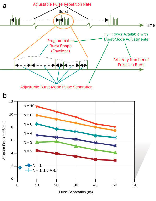
Figure 1. Pulse tailoring capability of a picosecond laser (a) and impact on micromachining ablation rate in silicon. N is the number of pulses in a burst, and repetition rate is 400 kHz, unless otherwise noted (b). Courtesy of MKS Spectra-Physics.
Pulse timing control is another key capability for improving machining throughput while retaining the cold-machining quality of picosecond lasers. Scanning galvanometers, or “galvos,” are commonly used for micromachining because of their ability to quickly accelerate the beam to very high speeds, but they are limited in the processing field of view, especially for small focus spots. Combining galvos with high-speed stages can result in fast processing over large areas.
To produce high-quality machining results, however, it is necessary to fire the laser at a constant spatial, not temporal,
separation over the entire motion trajectory. With some hybrid fiber lasers, pulses can be triggered on demand and synchronized with the motion profile — called position synchronized output (PSO) — with minimal timing jitter. This has been demonstrated using a picosecond hybrid fiber laser to process SnO2-coated glass with a variable speed motion trajectory.
Without PSO, ablation spot overlap increases as the motion slows, resulting in excessive burn, while with PSO, the laser-fired spots are evenly spaced around the entire trajectory (Figure 2a). The overall throughput advantage using PSO for a motion trajectory of a rounded corner rectangle — for example, a smartphone profile — with the typical acceleration of an industrial stage (5000 mm/s2 straight and 1000 mm/s2 cornering) can be quite dramatic (Figure 2b).
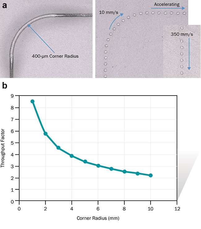
Figure 2. Variable trajectory speed processing with an IDL stage without PSO (a, left) versus with
PSO (a, right and inset). PSO throughput advantage versus corner radius for a 60- × 120-mm
rounded-corner rectangle (b). Courtesy of MKS Spectra-Physics.
Proliferating applications
With the recent advancements in picosecond laser technology along with dramatic improvements in reliability and cost of hybrid fiber laser technology, the adoption of picosecond lasers has expanded in a number of key applications. A few examples are highlighted here.
Printed circuit boards (PCBs) and circuits are ubiquitous in many large industries, such as consumer electronics and automotive. As electronic device densities increase, the drilling, cutting, and routing of PCBs, both rigid and flexible, have moved from mechanical processes to CO2 lasers to nanosecond UV and green lasers.
In the latest evolution to 5G mobile phones and wearables, flexible printed circuits (FPCs) require, in many cases, picosecond UV lasers to process the new and varied materials in these devices. One important material for 5G FPCs is liquid crystal polymer (LCP), a dielectric material well suited for high-speed radio frequency circuits. Both Cu/LCP/Cu laminates and bare LCP with picosecond UV lasers have been processed. For Cu/LCP/Cu, it was found that while both nanosecond UV and picosecond UV yield good quality, the features cut with picosecond pulses showed less debris and oxidation at the cut edge, which could be an important factor for downstream processes such as adhesion of patterned polyimide coverlay material.
For bare LCP, a straight line and contour cutting of 45-μm-thick material using a picosecond UV laser was demonstrated (Figure 3). The fastest process with best quality was achieved by using the pulse tailoring capability of a picosecond UV hybrid fiber laser to realize ~30% to 40% faster cuts than for a single pulse output.
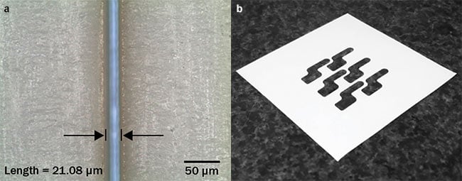
Figure 3. Picosecond UV laser cutting of 45-µm-thick liquid crystal polymer, straight cut at 500 mm/s (a), and contour cuts (b). Courtesy of MKS Spectra-Physics.
Flat panel displays, especially organic light-emitting diode (OLED) displays, require high-quality cutting of multiple layers of materials at high throughputs. Picosecond UV lasers are used for cutting
of these thermally sensitive materials, including polyimide, polyethylene terephthalate (PET), and polarizer films. High-quality cutting of polyimide and PET films using a picosecond UV hybrid fiber laser have also been demonstrated (Figure 4). High cutting speeds of up to 400 mm/s were achieved with this process.
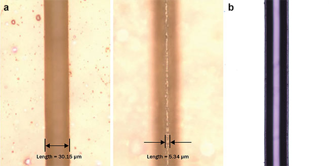
Figure 4. Picosecond UV laser cutting of polyimide (a) and polyethylene terephthalate (PET) films (b), which are commonly used in OLED displays. Courtesy of MKS Spectra-Physics.
Cutting brittle materials
Laser cutting of brittle materials such as glass, ceramics, and crystals is another important application for picosecond lasers. Traditional mechanical processes often cause severe cracking and chipping, especially for thinner materials, and require very low processing speeds to achieve acceptable yield. In many cases, nanosecond pulsed lasers offer good cost and performance for effectively machining these brittle materials. As manufacturers require higher machining quality and finer features, however, picosecond lasers are increasingly being adopted for machining such challenging materials.
For glass cutting, it was possible to cut 700-μm-thick aluminosilicate glass, commonly used as a cover glass for mobile devices, with a picosecond IR hybrid
fiber laser and a Bessel or nondiffracting beam optical setup to shape the beam.
The Bessel beam shaping optical components were chosen according to the systems described by Jan Jezek and
colleagues5, and Martí Duocastella and Craig Arnold6, with minor changes in focal lengths so as to demagnify the
Bessel beam length to approximately match the glass thickness. Best results were achieved using the hybrid fiber laser’s pulse tailoring capability to output a burst of two to four pulses with an intraburst pulse separation time of 10 ns. High-quality cutting results were realized with smooth-cut profiles and sidewalls with Ra ~0.25 to 0.30 μm (Figure 5).
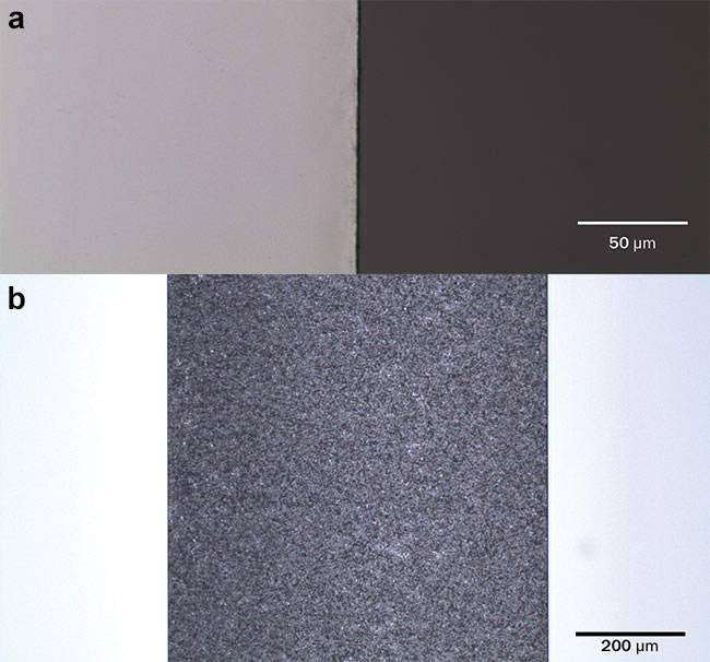
Figure 5. Optical microscope images showing the surface of aluminosilicate glass processed at 100-mm/s scan speed with a picosecond laser after mechanical cleaving of the glass (a). Optical microscope image showing cross section of aluminosilicate glass processed with a picosecond laser; roughness Ra is ~0.25 to 0.30 μm (b). Courtesy of MKS Spectra-Physics.
Picosecond lasers are also used for cutting sapphire and ceramics. Synthetic sapphire is used in mobile devices as a tough, scratch-resistant material for
camera windows and smartwatch faces, while ceramics are used for LED heat sinks, electronic device packages, and high-temperature PCBs. Using an IR picosecond laser, small disks were cut out of 150-µm-thick sapphire at high throughputs of ~1.5 seconds per 5 mm
diameter disk with no visible chipping and a smooth-cut edge (Figure 6a).
With the same picosecond laser, 5-mm-diameter holes could be cut in alumina ceramics at high speeds with high quality (Figure 6b).
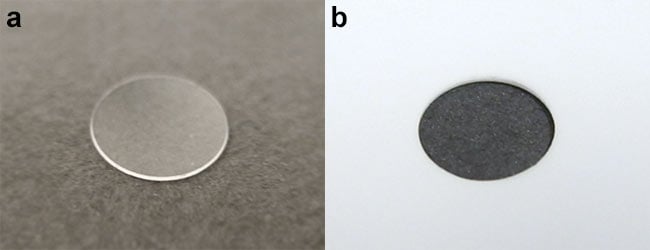
Figure 6. A 150-μm-thick sapphire disk cut with a picosecond laser (a), and a 200-μm-thick alumina ceramic hole (b). Courtesy of MKS Spectra-Physics.
Moving forward, a scaling of picosecond laser power at declining cost per watt may be realized, which will further drive rapid expansion into even more applications. With the capability to realize excellent micromachining results in critical materials at high speeds and ever lower costs, picosecond lasers have a very promising future.
Meet the authors
Herman Chui is senior director of product marketing for Spectra-Physics lasers at MKS Instruments; email: [email protected].
Jim Bovatsek is applications engineering manager for Spectra-Physics lasers at MKS Instruments; email: [email protected].
References
1. R.R. Gattass and E. Mazur (2008). Femtosecond laser micromachining in transparent materials. Nat Photonics, Vol. 2, Issue 4,
pp. 219-225.
2. X. Liu et al. (1997). Laser ablation and
micromachining with ultrashort laser pulses. IEEE J Quantum Electron, Vol. 33, Issue 10, pp. 1706-1716.
3. J. Bovatsek and R. Patel (2017). Ultrashort pulse laser technology for processing of advanced electronic materials. Proceedings of LPM2017. Toyama, Japan.
4. R. Patel et al. (2015). Doubling silicon ablation process efficiency and improving quality using high-power high repetition rate green laser with TimeShift capability.
J Laser Micro Nanoen, Vol. 10, Issue 2,
pp. 134-139.
5. J. Jezek et al. (2006). Formation of long and thin polymer fiber using nondiffracting beam. Opt Express, Vol. 14, Issue 19,
pp. 8506-8515.
6. M. Duocastella and C. Arnold (2012). Bessel and annular beams for materials processing. Laser Photonics Rev, Vol. 6, Issue 5,
pp. 607-621.