As global solar capacity increases, new materials and photovoltaic designs could deliver greater efficiency than conventional silicon cells, at a reasonable cost.
MICHAEL EISENSTEIN, SCIENCE WRITER
In a time of growing concern about climate change and the high cost of humanity’s carbon footprint, there are glimmers of hope. A global boom in sustainable energy investment is underway. The Renewable Energy Policy Network for the 21st Century (REN21) reports that in 2016, nearly a fifth of the world’s energy was derived from renewable sources. Solar energy is seeing particularly rapid growth. Between 2012 and 2017, global solar capacity more than quadrupled to a total of 402 gigawatts.
“I figure that by 2022, a third of our electricity in Australia is going to come from wind and solar,” said Martin Green, a leading researcher in solar photovoltaic (PV) technology at the University of New South Wales.

Specially designed achromatic lenses help concentrate light in a cutting-edge experimental CPV cell. Courtesy of Fraunhofer Institute for Solar Energy Systems.
Technology improvements have yielded steady gains in efficiency and falling costs per unit of energy generated, but exciting advancements in materials and PV design could help catapult solar power into an even more central role in global electrical grids.
Surpassing silicon
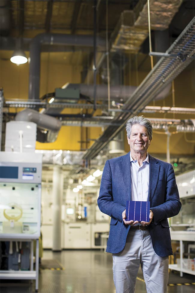
Almost all of today’s solar energy is generated by crystalline silicon-based PV cells — accounting for a 95% market share in 2017 — a technology that Green noted has remained largely unchanged since it was first developed in the 1970s. Recent years have seen a large uptick in the use of passivated emitter and rear cell (PERC) PVs, a design developed by Green and colleagues in 1989. PERC PVs provide a considerable boost in terms of the efficiency of light capture and power generation (Figure 1); however, they are still just a modified iteration of crystalline silicon solar cell technology. “Silicon’s position has become more dominant in
the fullness of time,” Green said. “It’s proving cheaper in production volumes, and the durability is really well established.”

Figure 1. Martin Green holds a PERC photovoltaic developed by his team at the University of New South Wales. Courtesy of UNSW Sydney and Anna Kucera.
This market dominance creates a
steep climb for competitors, but there are abundant opportunities to improve on the performance delivered by silicon cells. Among other metrics, PVs are judged by conversion efficiency, which represents the ratio of solar energy absorbed to the
electrical power generated. For any material, this efficiency is determined by
the Shockley-Queisser limit, a thermo-
dynamic calculation that accounts for
energetic loss as a result of radiative recombination and other factors. Silicon caps out at a limit of around 29% efficiency. Contemporary PVs have not yet reached that limit, but researchers are closing in fast. The current record for silicon is held by technology company Kaneka Corp., with an experimental
cell that delivered 26.6% conversion
efficiency.
Some manufacturers have opted to compete in terms of cost, and one way to achieve such savings is by formulating ultrathin semiconductors. For example, First Solar Inc. in Tempe, Ariz., has commercialized thin-film PVs based on cadmium telluride (CdTe). CdTe shares a similar crystalline structure to silicon and can be used to synthesize flexible thin films — 1/50th as thick as crystalline silicon wafers. This makes CdTe PVs more versatile and cheaper to manufacture, even if the efficiency of the technology remains low compared to silicon. First Solar’s current commercial modules deliver conversion efficiency on the order of 17% to 18%, but cost only 20 cents per watt generated to manufacture.
More recently, there has been a flurry of excitement around a class of minerals known as perovskites, which share a common structure with a naturally occurring form of calcium titanium oxide. “When you start substituting for the individual atoms, you can have perovskites with the same structure but all sorts of different
material properties,” said Chris Case, chief technology officer at Oxford PV Ltd., based in Oxford, England. His company is focused on developing hybrid cells that incorporate both organic methylammonium and inorganic lead halide chemical components.
According to Case, roughly half a million perovskites have been identified
to date, and research into the use of these materials for PV cells has yielded astonishingly rapid gains. “They went from zero to around 22% efficiency in only about five years,” said Green of the University of New South Wales. “That really shows that the material has some special properties.”
A layered solution
Perovskite PVs are certainly intriguing on their own, and Polish company Saule Technologies is exploring the potential of coating the exteriors of commercial
buildings with ink-jet-printed thin films of perovskite to power the offices within. But as with CdTe, silicon, and other promising semiconductor materials, the efficiency of single-layer cells is inevitably capped by the constraints of the Shockley-Queisser limit.
Any given PV material can respond only to a particular slice of the spectrum based on its bandgap properties, such that only photons with energy exceeding that bandgap can be absorbed. But Gerald Siefer of the Fraunhofer Institute for Solar Energy Systems noted that low bandgap
materials, which absorb a broader spectrum of photons, only generate weak voltages in return.
To make the most of the sun’s photonic riches, researchers are increasingly turning to tandem or multijunction designs, which incorporate stacks of multiple different semiconductor layers that slice the spectrum into manageable chunks. “You introduce a high bandgap cell that only absorbs high-energy photons, like 600 to 700 nm, then a solar cell with a medium bandgap that takes wavelength band up to maybe 900, and so on,” Siefer said. “These solar cells provide high voltage, but only take a part of the spectrum.”
The resulting tandem cells can thus greatly exceed the conversion efficiency of any one material.
This is a key element of Oxford PV’s strategy — making the most of perovskites by coupling them with workhorse silicon wafers within the context
of a tandem design. “A two-terminal,
two-junction tandem solar cell with silicon as the bottom cell and an optimally matched, wide-bandgap semiconductor
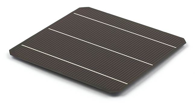
as the top cell has a combined peak efficiency of about 43%,” Case said. With their current tandem technology (Figure 2), the company is already reporting efficiency of 28% — just shy of the theoretical limit of silicon alone — and the company is moving rapidly toward commercial deployment.

Figure 2. A full-size version of Oxford PV’s perovskite-silicon tandem solar cell. Courtesy of Oxford PV.
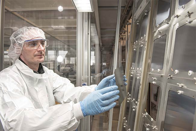
According to CEO Frank Averdung, Oxford PV has secured funding commitments on the order of $100 million, which it is investing toward a first-generation manufacturing facility (Figure 3) that
can produce PVs sufficient to generate 250 megawatts of power by the end of 2020. This tandem approach also allows the company to partner with the silicon PV industry rather than confronting it head on. “It’s technology disruption without business disruption,” Case said.

Figure 3. Production of tandem solar cells at Oxford PV’s pilot manufacturing facility. Courtesy of Oxford PV.
Green cautioned that perovskites are not without significant limitations and said many such PV compositions have proven too unstable for real-world use, with rapid degradation of performance relative to highly robust silicon. “You need a module that doesn’t degrade more than 2% after you do the worst things imaginable to it,” he said.
But Case is confident that Oxford’s formulation is up to the challenge, based on success in a series of accelerated stress tests involving exposure to various
environmental extremes. “We’ve passed those at the ‘minimodule’ level — single cells, basically,” he said.
The power of concentration
Since the 1990s, the satellites circling our planet have drawn power from an entirely different class of PVs based on III-V semiconductors. These materials take their name from the groups in the
periodic table within which their elemental components reside, and they include compounds such as gallium arsenide (GaAs) and indium phosphate (InP).
GaAs PVs currently deliver the highest confirmed performance of any single-junction solar cell — a 29.1% efficiency cell developed by Alta Devices in Sunnyvale, Calif. These cells have a theoretical efficiency limit on the order of 33.5% (much higher if coupled with other materials) and have proven remarkably
durable even in the harsh realm of outer space. “You have all this radiation from the sun that can degrade materials, and the degradation from III-V multijunction cells is lower than for standard silicon cells,” Fraunhofer’s Siefer said. “That is why these cells have completely taken over the market in space.” As with the perovskites, he said, these materials also offer a broad palette of materials from which to choose, allowing manufactures to perform “bandgap engineering” to assemble multijunction PVs that harvest solar energy with unprecedented efficiency.
But bringing the prices of these materials back down to Earth has proven a tough feat, largely because of the high cost of manufacturing and the relative scarcity of elements such as gallium and indium. For a conventional terrestrial solar panel, Siefer estimates that the use of III-V
materials would boost costs by as much
as 100- to 200-fold.

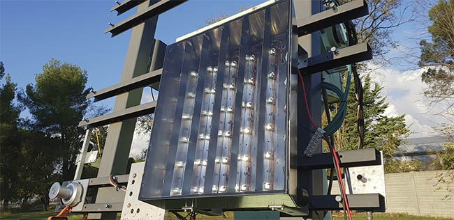
Figure 4. III-V materials are too expensive for large-scale cell production, but can be combined with lenses that focus the sunlight to extract more energy from less real estate. Courtesy of Fraunhofer Institute for Solar Energy Systems.
He and his colleagues at Fraunhofer have demonstrated a potentially cost-effective solution, based on a concentrator photovoltaic (CPV) design, as part of the recently concluded European CPVMatch consortium (Figures 4 and 5). “The idea is that you use a larger lens or mirror to focus the sun’s light onto a tiny solar cell,” Siefer said. This would then be attached to a tracking system, which reorients the CPV to maintain maximal light exposure. Using cutting-edge optics developed at the University of Madrid, and components developed by other industry and academic partners, the consortium produced an experimental CPV module with a conversion efficiency of 41.4%.

Figure 5. Mirror modules offer an alternative approach for focusing light in a CPV cell design. Courtesy of Fraunhofer Institute for Solar Energy Systems.
This was purely a proof-of-concept demonstration. Siefer said commercialization is still a way off.
Indeed, many companies working in the CPV space have shuttered their doors or changed their priorities in recent years. But he also believes this technology could fill a valuable niche, noting that although the costs of manufacturing are higher, they are not prohibitively so, and the actual carbon footprint of producing CPVs is severalfold lower than for silicon panels.
Furthermore, the smaller CPV systems have a far smaller footprint, which means they could potentially be installed in settings where land is already being used for other purposes such as agriculture, rather than conquering the landscape as a conventional solar panel array might.
[email protected]