The need for lighter-weight soldier systems and unmanned aerial systems is prompting dramatic SWaP reductions in photonic gear, without sacrificing performance.
G. SCOTT LIBONATE, JENOPTIK OPTICAL SYSTEMS LLC
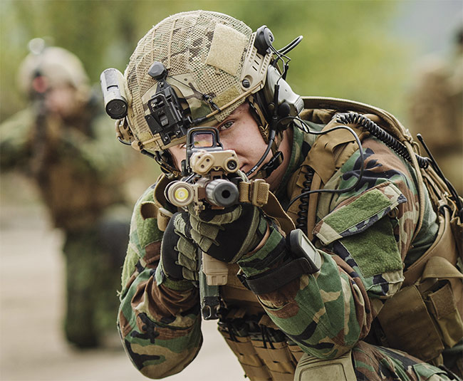
Many modern troops go to battle carrying up to 80 lbs of gear per soldier. Approximately 20 lbs of this weight can come from batteries for radios and electro-optics. Reducing a soldier’s burden improves mobility and mission effectiveness and reduces fatigue and repetitive stress injuries. Unmanned aerial systems (UASs), or drones, are meanwhile becoming standard-issue gear, and the size, weight, and power (SWaP) of electro-optic payloads has a direct impact on the portability of these platforms.

Courtesy of JENOPTIK.
Recent advancements in the efficiency of light sources, reductions in sensor and display pixel sizes, and the use of next-generation optics have all converged to facilitate a new generation of military photonic systems that deliver increased capabilities and enhanced performance, all at reduced SWaP.
Why SWaP is vital
Since the Vietnam War, U.S. soldiers have entered new combat theaters equipped with an ever-growing array of electro-optical gear, ranging from night-vision goggles and weapon-mounted lasers to rangefinders and targeting devices. More recent modernization efforts aim to achieve the seemingly contradictory goals of enhancing capabilities while simultaneously reducing the soldier’s burden. Current focuses include increasing troops’ lethality by enhancing their situational awareness, providing them with access to the tactical battlefield network, and employing rapid target acquisition technologies. Such capabilities would enable squads to observe enemy activity at greater distances to allow for making initial contact under optimal conditions and to ensure greater agility as squads maneuver to gain positions of advantage.
Drones, which are instrumental to these goals, have become an increasingly common addition to the soldier’s electro-optic arsenal, and there is intense pressure to evolve drone capabilities while reducing their SWaP profile. There is a general trend toward fielding larger quantities of smaller UASs to provide local reconnaissance. In a typical scenario, soldiers would pull a nano drone out of their packs and send it to look over the next hill. The desire is for the drones to provide high-resolution video and facilitate the addition of other payloads if a mission calls for it.

A nonrotationally symmetric freeform lens is used to shape a collimated beam to project a logo. This is a simple example of freeform optical fabrication techniques that allow for the generation of any optical surface and can be used to combine multiple traditional optics into a single freeform element. Courtesy of JENOPTIK.
Interestingly, the consumer sector is contributing solutions to the defense industry’s SWaP challenges. Extreme market competition in the gaming, virtual and augmented reality, smartphone, telecom, and autonomous vehicle industries has dramatically increased electronic processing capabilities while driving down component footprint and power consumption. This competition has led to advancements in emitter, sensor, and display technologies, as well as to the development of new competing technologies with expanded capabilities.
As a result, the defense industry’s
electro-optic payload designers have a wider array of component options to choose from that did not exist several years ago. The broader variety of component options also facilitates the design and integration of more compact, more efficient, and higher-performing systems. Meanwhile, optical and optomechanical fabrication techniques have also advanced, which allows designers to replace conventional optics with nontraditional optics to further reduce the size and weight of optical subassemblies.
Emitters diversify options
Active systems such as illuminators, aim lasers, laser rangefinders, lidar, and target designators have all benefited from the improved wall-plug efficiency for today’s light sources, as well as from improvements in beam quality and a growing variety of sources. Flashlights provide a simple example of this trend: Once reliant on light bulbs that quickly consumed the energy stored in D-cell batteries, flashlights now rely on more efficient LEDs that are able to operate longer when powered by a AAA battery. LED flashlights also deliver brighter, more uniform illumination.
Decades ago, designers might have also been forced to combine an incandescent source with bandpass filters to generate a red, near-infrared (NIR), or shortwave IR (SWIR) illuminator or beacon — an approach that wasted a large fraction of the available light. Now, there are edge-emitting laser diodes, light-emitting diodes, vertical-cavity surface-emitting lasers (VCSELs), diode-pumped solid-state lasers, quantum cascade lasers, and fiber lasers that span a range of sizes, power draws, costs, wavelengths and bandwidths, beam qualities, output powers, pulse widths, and pulse repetition frequencies. The result is that designers have more freedom to select the optimal set of characteristics for their specific application.
The advent of new emitter technologies has improved SWaP options in manifold ways. In addition to higher efficiency, there are indirect improvements. When spectral and beam characteristics of the source are better matched to the demands of the application, the result is less wasted light. This, in turn, reduces waste heat, which then reduces required thermal mass and cooling requirements and multiplies the improvements in the SWaP profile.
Commercial sector help
In addition to improvements in the speed, power efficiency, and read noise of camera electronics, sensor pixel sizes have been decreasing with a corresponding increase in the number of pixels. This trend has been largely driven by the cellphone industry and has been most evident in visible cameras, but it is also evident in SWIR and thermal cameras.
Smaller pixels within a given pixel-
array format allow the use of smaller optics, while larger camera formats can support digital electronic zoom (e-zoom) and electronic image stabilization approaches in lieu of their optical counterparts. These options can reduce the complexity of camera optics and thus their size and weight.
After visible cameras, thermal imagers have seen the most dramatic SWaP improvements, along with more moderate costs. Both have resulted from the availability of new materials and the technology’s entry into commercial markets.
Suppliers such as FLIR Systems
and Seek Thermal offer compact, low-resolution cameras to the commercial markets at low cost, and the process
and material enhancements that their cameras leverage have benefitted military technology as well.
The reduction in the SWaP of uncooled thermal cameras achieved in the last decade is exemplified by comparing two of JENOPTIK’s thermal camera offerings: Blackbird and its recently released
successor, EVIDIR. Blackbird measured
125 × 90 × 95 mm and weighed over
900 g, while EVIDIR measures only 20 × 29 × 31 mm, weighs 45 g, and provides all the same features along with improved performance. EVIDIR draws less than 800 mW of power and has less than
40 mK NETD (noise equivalent temperature difference).
Like thermal imagers, mid-wavelength IR (MWIR) systems have exhibited similar improvements in pixel size and high-definition formats. But the growth of the systems has been limited to high-end applications due to higher costs, and to larger platforms due to the need for cryogenic cooling, which increases the systems’ SWaP profile.
Optics options multiply
Modern optical fabrication techniques now facilitate the generation of nearly any imaginable optical surface and could theoretically allow the combination of an entire optical assembly into a single freeform element. The use of polymer freeform surfaces has increased in recent years, in markets such as automotive, lighting, energy, and medical and sensor technologies. But aside from aspheres, defense designers have yet to take full advantage of the promise of freeform optics.
Meanwhile, other nontraditional optical technologies are also beginning to gain acceptance but have not yet proliferated widely. These include microlens arrays, diffractive optical elements, and geometrical phase optics (aka waveplate lenses or 4G optics).
Microlens arrays are most commonly used to increase the optical fill factor in sensor arrays to enhance array sensitivity. The material properties for some sensor materials permit the growth of lenslets in situ as part of the wafer fab process — an approach that reduces cost.
Diffractive optical elements can similarly improve performance while reducing SWaP. Ideal for allowing laser systems to achieve uniform performance over large areas, they are most commonly used for pattern generators, homogenizers/diffusers, beamsplitters, beam shapers, and coherent recombiners in systems that target fields such as remote sensing and lidar.
4G optics promise intriguing options for minimizing system SWaP profiles, but they have yet to be readily adopted due to their unfamiliarity and high initial unit costs. The technology makes use of the phase difference between the extraordinary and ordinary rays in birefringent materials and variations in anisotropy axis orientation to replicate nearly any optic. BEAM Co. in Orlando, Fla., for example, uses photoalignment techniques to lock liquid crystal molecules into custom patterns on a polymer film bonded to glass. This allows the designer to replace traditional optics with a stack of low-SWaP glass plates that can also be designed to be made switchable. Tunable liquid crystal cells can be added in series to allow optics to be switched on and off with no moving parts. This allows stepwise switchable zoom assemblies, switchable beamsplitters that fold beams into and out of an optical path, or variable beam directors for laser beam or image stabilization.
Display sector
The importance of high-resolution, low-power displays has grown because the imaging systems that are integrated into tactical battlefield networks must clearly display and differentiate between augmented reality symbology and external imagery, while also hosting native system imagery. As with sensors, display pixel sizes are decreasing, which allows similar reductions in the size of eyepiece optics. Liquid crystal and OLED displays have dominated the market to date, but micro-LED displays may prove to be a better alternative because they can improve the low-power operation of liquid crystal displays, yet maintain the high brightness and contrast of OLED displays.
Future directions
As commercial markets drive down component costs, the consolidation of previously disparate systems becomes more acceptable cost-wise. Such system-level consolidations compound SWaP reductions by eliminating the number of multiple devices with individual sets of batteries, displays, user interfaces, and mechanical interconnects. For example, high-operating-temperature MWIR cameras, which are able to see most battlefield lasers, could permit the ability to replace separate SWIR and thermal cameras with a single device in some applications. Similarly, the U.S. Army is developing a new fire-control device for small arms that combines riflescope, laser rangefinder, ballistic calculator, and disturbed reticle into a single-target engagement device.
Further, the latest night-vision goggles combine image intensifiers with a thermal imager and augmented reality.
In spite of such advancements, the biggest capability gap remains in night-vision technology. Night-vision goggles are heavy and bulky and not amenable to interfacing with tactical networks. There is a strong desire for digital NIR cameras with sensitivity, resolution, and cost comparable to current night-vision goggles. But the power demand and costs are high, and digital imaging options such as intensified CMOS or CCD cameras or electron-bombarded active-pixel sensor cameras have been unable to gain user acceptance.
While component advancements have generally been beneficial, the proliferation of high-quality commercial technology sensitive in the NIR has reduced our military’s dominance in night operations and forced soldiers to change tactics to avoid actively emitting in the NIR until they start firing. There is a push to move into other technologies to regain the nighttime technical advantage.

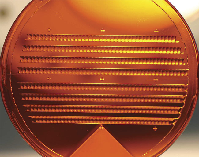
A custom 50-mm-diameter gallium phosphide microlens array used for collimation of individual emitters in an infrared laser array. The ability to place multiple custom lenses together in a small space at high tolerances facilitates extremely compact form factors. Courtesy of JENOPTIK.
Recent advancements in photonic components have simultaneously improved both performance and SWaP profiles for military electro-optics systems. Further SWaP enhancements will be accrued through continued consolidation of previously disparate functionalities into single systems. Furthermore, there will be a drive to fill capability gaps and maintain technological overmatch. As the resulting technology becomes more complex, reducing the soldier’s cognitive load through means such as AI will become as important as reducing physical load.
Meet the author
G. Scott Libonate is North American director of advanced systems for JENOPTIK Optical Systems LLC. He received a doctorate in infrared astrophysics from the University of Rochester and has a background in military camera and laser systems.
Rangefinder SWaP Continues to Evolve
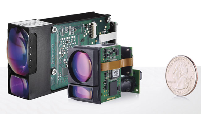
JENOPTIK’s DLEM line of laser rangefinder modules serves as a good example of the rapid evolution timeline of size, weight, and power (SWaP) enhancements in military electro-optic systems. DLEM modules are compact, 1550-nm diode laser rangefinders
designed for incorporation into targeting devices and drone payloads.

The subsequent generations of JENOPTIK’s DLEM laser rangefinders offer one example of how size, weight, and power (SWaP) profiles evolve over time. Optics, power efficiency, and algorithm enhancements have enabled significant reductions in this 1500-m class microrangefinder product in less than 10 years. Courtesy of JENOPTIK.
Initially, the most compact product of the line was the DLEM 1k. It was replaced by
the DLEM SR, which was in turn replaced by the DLEM 20. Advancements in commercially viable optics technologies facilitated new optics concepts that improved beam quality at reduced aperture. Coupled with improvements to algorithms and to the power efficiency of electronics, this led to dramatic reductions in SWaP with each new generation of these microrangefinders, without degrading their performance (see table). The trend is continuing with the release of two more enhanced versions of the product — one smaller in size and one with increased range — in 2021.
Evolution of SWaP in Rangefinder Generations
