Graphene holds great potential for a variety of applications, from photovoltaics to lasers and sensors.
Two-dimensional materials could soon provide useful photonic solutions for our 3-D world. Graphene – a single layer of carbon – might find a home in displays, detectors and modulators. Along with other monolayer materials such as molybdenum disulfide, it could improve optical communication links, sensors and other devices. Commercial manufacturing of these flat materials is a challenge, but there are claims of successful solutions.
Of the 2-D materials, graphene has attracted the most attention. Consisting of carbon atoms arranged in a honeycomb lattice, graphene’s electrical conductivity is better than that of copper; its electron mobility far outpaces silicon. Initially investigated for use in electronics, its true value may lie elsewhere.
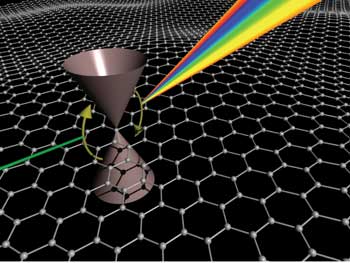
Graphene can modulate light of any wavelength, and this broadband capability makes the material useful as a saturable absorber. Photo courtesy of University of Cambridge Graphene Center.
“The real potential for graphene is in photonics,” said Andrea C. Ferrari, a professor of nanotechnology at the University of Cambridge in England. He heads the graphene photonics and optoelectronics section, and is chairman of the executive board of the Graphene Flagship, a just-launched, billion-euro, 10-year European 2-D material research initiative.
Ferrari was co-author of a 2010 Nature Photonics paper that pointed to graphene being useful in photonics as a transparent conductor, in photovoltaic and light-emitting devices, in photodetectors, and in saturable absorbers and ultrafast lasers. The basic research demonstrating these applications has now been done, and the results are promising, he said.
For instance, single-layer graphene absorbs only 2.3 percent of the visible light passing through it, making it a transparent conductor. These are found in smartphone and touch-screen displays, a multimillion-unit yearly market. Currently, the transparent conductor indium tin oxide (ITO) is used in these displays, but graphene could potentially replace it.
“In transparent conductors, it is already there, competing with ITO in terms of properties and performance. In terms of bendability and flexibility, it far outperforms ITO,” Ferrari said.
Korea’s Samsung, a leading phone maker, has demonstrated a prototype device with a graphene-based display. As of late 2013, though, graphene-based phones are not yet widely available.
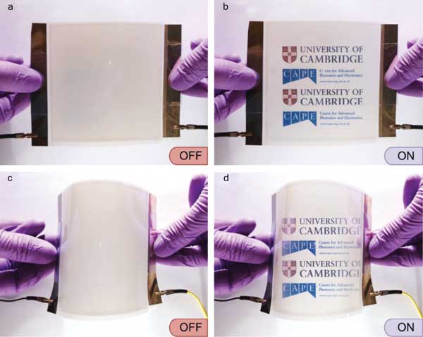
A graphene-based flexible smart window prototype in operation. Photo courtesy of University of Cambridge Graphene Center.
The transparency of graphene is a plus in a display. However, the low absorption is a minus when it comes to making a photodetector or a solar cell. From the visible through the near-IR, graphene absorbs only about one-fiftieth of the light that strikes it.
Researchers are working on several ways to boost that number. Investigators at IBM’s T.J. Watson Research Center in Yorktown Heights, N.Y., for instance, found that graphene soaks up photons more readily at longer wavelengths. “Beyond the near-infrared, we found that graphene can absorb a lot more light and detect it, particularly in the terahertz regime,” said Phaedon Avouris, an IBM fellow and manager of nanometer science and technology. He is co-author of a 2013 Nature Communications paper on the research.
In the terahertz, the absorption can be as high as 40 percent, Avouris added. It can be further enhanced through the use of plasmons, collective electronic oscillations tunable via an external voltage. Plasmons can boost the photodetector signal by as much as 1500 percent, with coupling of the light into the plasmons achieved by patterning the material into microscopic ribbons, rings and other nanostructures.
One difference between graphene plasmons and those of gold or other noble metals could be longevity. In metals, plasmons decay quickly. That may not be the case with graphene, and IBM researchers are investigating the implications.
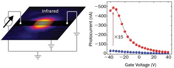
For photodetectors, graphene photon absorption must be large and tunable. Here, voltage-dependent graphene absorption of IR is enhanced by plasmons excited by properly polarized light (red) versus light not so polarized (blue). Courtesy of Nature Communications.
As for the material’s future, existing terahertz detectors depend upon low temperatures, Avouris said. In contrast, graphene photodetectors could work at room temperature, would be composed of inexpensive carbon, and could be made in large areas – all key advantages for security and other applications.
Increasing the interaction of graphene and light is a research focus of Dirk Englund, an assistant professor of electrical engineering and computer science at MIT in Cambridge, Mass. His goal is to get the number close to 100 percent in a spectrally tunable way.
Early work showed that graphene could make fast photodetectors, potentially enabling detection and modulation in excess of 500 GHz, Englund said. However, the material’s low absorption results in little photocurrent being generated per watt of incoming light. This meager response is one barrier to actually putting graphene to work in optical communications or other applications.
There are several ways to get close to complete absorption, Englund said. His group has investigated the integration of graphene with a planar photonic crystal. By adjusting a voltage applied to the graphene, the researchers showed in a 2013 Nano Letters paper that it was possible to change the reflectivity of the cavity by 10 dB, or tenfold. That’s enough modulation amplitude for many optical communication schemes, Englund said.
Devices built using this approach would be small and have little capacitance. That would allow them to switch states quickly and thereby transmit at high rates. They also would have other desirable characteristics. “You could make a modulator that is very, very compact and also has very low energy consumption,” Englund said.
Another technique that ups absorption involves the use of a silicon waveguide. Recently, researchers integrated graphene for about 50 µm along a waveguide’s face. The interaction between the two materials effectively turned the graphene on edge to the incoming light and thereby produced nearly complete absorption.
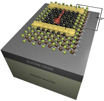
A hybrid device consisting of graphene (dark spheres) and molybdenum disulfide has sensitivity a billion times that of a silicon photodetector. Photo courtesy of Arindam Ghosh, Indian Institute of Science.
Graphene also could be used in conjunction with other materials. In particular, molybdenum disulfide, or MoS2, is seen as promising for photonics. Single layers of the material readily generate photocurrent when illuminated by visible light. The effect can be enhanced through the use of graphene as a transparent conductor, according to a 2013 Nature Nanotechnology report.
The paper’s co-author, Arindam Ghosh, an associate physics professor at the Indian Institute of Science in Bangalore, said that when light strikes molybdenum disulfide, photoelectrons are generated, but these have trouble getting out because the material is a poor conductor. To overcome this, his group constructed a hybrid device, with graphene in intimate contact with the photosensitive molybdenum disulfide. With the application of the appropriate voltage, light-generated electrons are swept into the graphene – provided that a critical boundary is clean.
“If the interface is not very good and there is plenty of dirt or imperfections at the interface, the electrons simply wouldn’t go – and you lose all of the effect,” Ghosh said.
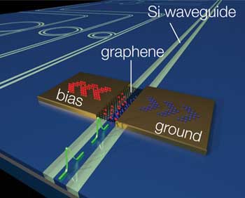
Integration of graphene with a silicon waveguide enhances absorption and creates a photodetector. Photo courtesy of Dirk Englund, MIT.
A key innovation was the development of a method to create a pristine interface, he added. The group found that the hybrid device is about a billion times more sensitive in terms of current generated per watt of illumination than silicon. Ghosh said a meter-square hybrid device could detect a candle 100,000 km away – almost a third the distance from Earth to the moon.
The researchers’ proof-of-concept device illustrates what may be the biggest problem facing graphene and other 2-D materials: manufacturing. The hybrid was built by using tape to mechanically exfoliate graphene and molybdenum disulfide. The atomically flat films were then physically attached and heated. The process is simple but ill-suited to commercial manufacturing because it starts by mechanically peeling off high-quality but very small layers of material.
Recognizing that, researchers and the emerging graphene industry have turned to chemical vapor deposition. The method vaporizes carbon or other appropriate materials and puts down needed layers on a substrate, such as copper, sapphire and silicon carbide. Copper, the substrate of choice for producing graphene, is heated to 1000 °C, while the other two may require temperatures up to 1500 °C. After deposition, the graphene layer then is transferred from the initial to the final substrate, which could be glass, plastic or silicon. Making the process and resulting product commercially viable has proved difficult.
Different applications demand different graphene quality levels and cost targets, said Bruce Willner, chief science officer for Graphene Frontiers of Philadelphia. Besides supplying material for use by others, the company is working on a line of graphene-powered chemical and biological sensors.
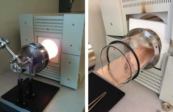
Chemical vapor deposition of graphene on a copper substrate ((left) during the process and (right) after) is seen as a promising way to manufacture graphene for commercial applications. Photo courtesy of Graphene Frontiers.
Some applications, such as transparent conductors for displays, require a lot of lower-quality and inexpensive graphene.
In contrast, transistors need small amounts of very high quality graphene, which can be more costly. Still other applications, such as biosensors, require similar quantities of lesser-quality material. These manufacturing-related specifications apply to the film after transfer to the ultimate substrate.
Graphene Frontiers has made significant progress in satisfying these demands, Willner said. The company’s process involves a copper substrate that is reused, helping keep costs down. Today it can yield polycrystalline films as large as
60 in.; by next year, it expects to demonstrate an in-line, roll-to-roll graphene chemical vapor deposition process suitable for high-volume, lower-quality film applications, he said.
As for sensors, he said that the company’s process today results in roughly 100-µm-wide areas of single crystal graphene, big enough for commercial applications. Importantly, the transfer process doesn’t leave behind performance-robbing residue. The company feels it is on its way to a workable solution for making graphene of appropriate quality and cost. The cleanliness of the film and interface meets important requirements.
“We think it is quite clean – certainly clean enough for sensors,” Willner said.