GUENTER HUMMELT, NANOSYSTEC GMBH
Optoelectronic components are designed with an almost unlimited number of variations. Consequently, each device requires a unique packaging process. Component manufacturers are asking for an ever-increasing level of automation to meet their cost and quality objectives, and the time between prototyping and high-yield volume production should be kept as short as possible.
Aligning and joining these devices with laser welding, laser soldering or epoxy gluing is no easy task. The manufacturing equipment must cope with this variety and complexity while needing to address contradictory requirements. The system must be versatile and should produce various devices with different mechanical, optical and electrical features. The key challenge is the combination of the shortest possible alignment and assembly time with maximum coupling efficiency.

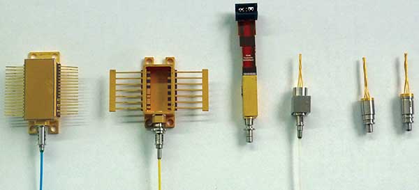
A small selection of optoelectronic devices to be produced on the same alignment and laser welding station. Courtesy of Nanosystec GmbH.
One of the important considerations during the design of a device is to verify that the process flow has a logical structure. After each manufacturing step, performance checks should be executable. The earlier a nonconforming component is identified, the faster corrective measures can be initiated, or the component can be rejected in order to save precious production time. If the necessary levels for important values are not met, the device should not be moved to the next production step. Examples of such values are optical power, power stability, beam pointing, mechanical tolerances and loss during welding or epoxy gluing.
Designers may find it beneficial to discuss the process steps below with an equipment manufacturer during this early development stage. Such discussions could lead to a device and machine design that is well-suited for efficient production, setting the stage for a rapid transfer from development to mass production.
Device-specific trays decrease cycle time
A tray concept shifts a large portion of the handling time from the manufacturing system to an external loading station and provides a versatile machine interface for different devices or process steps. Such trays accommodate all kinds of different devices and housings without the need to change the system hardware. Devices of any shape and size are mechanically gripped and firmly held in place.
The electrical interface between the tray and the production station allows for the control of the device functions, such as laser and receiver channels, thermoelectric cooling elements, and modulators. By assigning the signals to the respective pins and switching them automatically from the process, a change between different devices takes minimal time.
To increase capacity, the station works with two identical trays for one device type. One is processed automatically inside the system while the second is loaded on an external loading station. Depending on the assembly procedure, trays loaded with multiple devices can be used to further reduce the handling time. The loading station is used to bring the devices into their starting position for pre-alignment.
For a fully automated process to be justifiable, loading and unloading needs to take a substantial amount of the cycle time. Only processes that run less than 30 seconds with another 10 to 15 seconds handling time call for this level of automation. One example of such a high-volume product is the alignment and welding of a transistor outline (TO) can with a receptacle.
If optical fibers are attached and need to be connected during the alignment procedure, automation becomes more difficult. However, intelligent concepts with trays that hold multiple device sets could provide a good compromise between single-set loading and full automation at reasonable costs. Packaging efficiency could also be impeded by several factors associated with the devices. For example, variations in the dimensions of the parts complicate a repeatable gripping process. Other impediments to efficiency include the positioning of electrical connecting pins or pads that are not specified by the manufacturer with suitable tolerances, and varying tolerances between manufacturing batches. For joints with laser welding, an excellent and consistent surface quality is paramount.

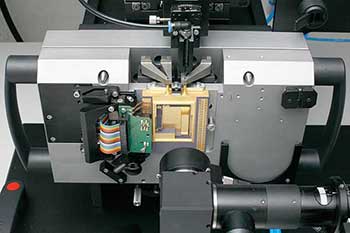
An external loading station for the pre-alignment of two optical fibers has two advantages: 1. The loading/unloading takes place while a second tray is automatically processed inside the production system. 2. The pre-alignment of the fibers (rotation and Z distance) reduces cycle time in the workstation. Courtesy of Nanosystec GmbH.
Minimize alignment times
A good start position of the devices to be aligned reduces the search area in which the effective command variable is captured before the optimization starts. Important time is often wasted during this pre-alignment.
The manufacturing equipment uses mechanical references of the device in order to define the positions of the various parts in space. Depending on the device types, machine vision algorithms support this mechanical referencing for pick-up procedures with grippers. Vacuum channels in the gripper jaws guarantee a repeatable gripping position. The optical path should be found relative to reference marks or characteristic features with the smallest possible deviation. Inevitable tolerances have to be compensated by the search algorithm for the first signal. For example, a spiral search perpendicular to the optical axis looks for maximum photo detector current from an external or internal photodiode.
After this first signal is found, the channel will be optimized for maximum coupling efficiency and signal strength in linear X, Y and Z directions. Additional routines such as polarization extinction ratio around the optical axis or angular alignment in pitch and yaw might follow. Multichannel devices, such as multiple wavelength devices, programmable logic controllers (PLCs) or splitters, need further optimization to ensure the desired coupling efficiency in all channels.
To achieve the optimum position, the signal should be free from fluctuations and side maxima. The more disturbing influences occur during the alignment, the longer the optimization process takes, expending costly machine time.
State-of-the-art systems can achieve an alignment repeatability below 100 nm in linear direction and below 0.0005° in rotary direction. This high accuracy ensures that the optimum position is consistent and perfect. Possible errors and inconsistencies can be reduced to device characteristics.
Laser welding vs. epoxy gluing
Having reached the ideal coupling characteristics, the position between the parts to be joined should be maintained without shift during the final assembly with laser welding or epoxy gluing.
Laser welding is the most expensive, fastest and most durable procedure with the highest mechanical strength. It requires metal parts that are suitable for laser welding and that have an excellent and consistent surface quality. There should be no gap between the parts to be joined as this leads to unwanted mechanical shift and subsequent loss of coupling efficiency. The weld spot pattern needs to be adapted to the device geometry in order to keep the position with a deviation in the submicrometer range.
Auxiliary parts such as sleeves, weld clips and brackets require tight mechanical tolerances to provide consistent results. The weld laser energy is divided into two or three single beams, which deliver the same amount of energy into the same spot size. Setting the splitting ratio and weld spot diameter/focus position to the exact same value for all beams reduces the weld shift to a minimum.
For the so-called coaxial devices, the parts to be joined, such as a butterfly, gigabit passive optical network (GPON) or laser diode housing, are brought into a parallel position without any gap. A half sphere floating on an air cushion is an ideal and fast method to achieve this requirement. Ideally the two surfaces of the two components are perfectly perpendicular to the mechanical and optical central axis. In reality this is not the case due to inevitable manufacturing tolerances. The half sphere works without friction and the part carried by the gripper of the half sphere orients itself perfectly to the opposing surface. With this technique, the position is maintained during the welding, and time-consuming corrective methods can be avoided. The machining quality of the devices is very important to avoid tilt due to bumps, scratches or ball-shaped surfaces.

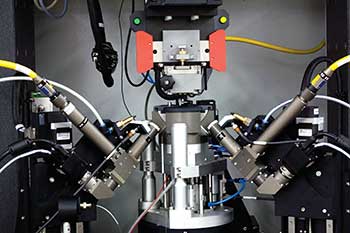
During laser welding of coaxial devices, a perfect surface contact over the entire area avoids weld shift. A half sphere floating on an air cushion allows for a fast and accurate mating. Courtesy of Nanosystec GmbH.
Linear devices, as in optics or fibers inside a butterfly or similar package, are assembled using weld clips and brackets. The automated placement of the weld clip, which is taken from a planar pick-up position, leads to repeatable weld results because both sides of the clip evenly touch the base. As the shift occurs always in the same direction, offset values help to minimize the shift. The inevitable excess shift is corrected with a gentle bending procedure.
The tolerances of the fiber ferrules and clips determine the amount of correction. With good tolerances, little power is lost during laser welding and a gentle bending procedure brings the device back to optimum coupling efficiency. If the tolerances are not tight enough, the signal can completely vanish, leading to a difficult procedure to pull the coupling efficiency back. This procedure is not only time-consuming, but it also introduces a large amount of mechanical stress due to the large bending area.
Compared to laser welding, gluing is more forgiving regarding the mechanical tolerances because gaps between components are filled with glue. Different materials can be glued and there is no need for metallic sockets. During the curing procedure, the glue shrinks. Depending on the resin, this curing procedure takes several seconds to minutes, wasting valuable time. Typical devices that use epoxy gluing are collimating, steering and focusing lenses, lens arrays, splitters and modulators with single or multichannel fiber arrays, as well as PLCs.
The requirements for the part tolerance are not as tight as for laser welding. However, the size of the gap influences the corrective offset according to the shrinkage of the resin. In order to maintain the optimum position, the right offset for the thickness of the resin has to be chosen and ideally the gap should be similar from device to device. This will result in stable manufacturing parameters and a consistently good performance.
Uniform dispensing of the resin is important as well. This is true not only for the amount but also for the position of the resin. Curing with UV, either from arc lamps or LED sources, finalizes the process. In most cases curing is continued outside the production system with elevated temperatures over several hours.

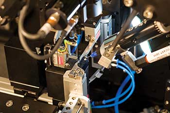
The precise positioning of the optics as well as the accurate dispensing and curing procedure determine the final performance. Courtesy of Nanosystec GmbH.
The path to full automation
The systems described above are operating semiautomatically. Loading and unloading requires operators while the process itself is automatic. Loading and unloading time is reduced by the use of trays or by cartridges carrying several sets of components.
To increase manufacturing speed further, the time for loading and unloading has to be reduced and the process itself needs to run faster. As stated above, the devices have to be designed in a way that is suitable for automation. Another strong requirement is a high degree
of uniformity for the parts used. Deviations in shape, size and optical characteristic negatively impact the automated process.
Fully automated alignment and welding systems are under development. The parts to be aligned and permanently attached are delivered to the system in cartridges holding up to 50 pieces and the finished parts are collected in magazines. In addition, new alignment concepts will reduce the cycle time substantially.
In order to utilize the advantages of the CMOS production process for silicon waveguides, the alignment and gluing process of optical fibers requires even shorter processing times. By accepting larger losses, passive alignment of the fibers provides another approach. The optical fiber has to be placed with an accuracy of a few micrometers in front of the chip. As dispensing of the resin and curing takes several seconds per connection, the simultaneous attachment of several fibers decreases the process time.
Meet the author
Guenter Hummelt is the CTO of Nanosystec GmbH in Gross-Umstadt, Germany; email: [email protected].