Once an exotic application of femtosecond lasers, terahertz sensing is now a preferred method for nondestructive analysis, with use cases in the automotive industry.
LARS LIEBERMEISTER AND ROBERT KOHLHAAS FRAUNHOFER HHI, AND ANDREAS THOSS CONTRIBUTING EDITOR
The terahertz portion of the electromagnetic spectrum refers to the frequencies between ~100 GHz and
~10 THz. This corresponds to wavelengths between
3 mm and 30 µm.
Lying between the electronic realm at lower frequencies and the optical (infrared) part of the spectrum — in effect, between two worlds — terahertz radiation has historically been difficult to generate. The efficiency of electronic devices, for example, transistors and oscillators, drops sharply as frequencies increase into the terahertz range. Photonic devices work well at higher (infrared and visible light) frequencies, but they struggle to produce
terahertz radiation due to the need for highly precise and stable frequency
mixing or efficient nonlinear optical
processes. This bottleneck is the origin
of the familiar term “terahertz gap.”
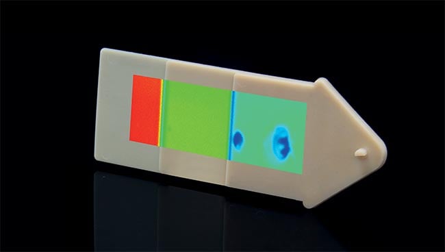
Courtesy of TOPTICA Photonics.
Moreover, terahertz radiation has low photon energy (in the range of milli-electronvolts), which makes it challenging to detect and generate efficiently. At the same time, this low photon energy makes terahertz radiation nonionizing and safe for humans.
The use of quantum cascade lasers offers one seemingly conventional method for generating terahertz radiation. However, these sources require cooling
to cryogenic temperatures to reduce noise and achieve stable output, which can complicate and restrict their practical application.
Other techniques involve complex
and expensive equipment, such as free-electron lasers and/or large-scale accelerator facilities. These devices and systems are more obviously unfeasible for widespread use.
Nevertheless, terahertz technology is on the rise, especially in the domain of sensing and due to optoelectronic solutions. Much like legacy terahertz radiation sources, the basic functions and prospects for these emerging solutions promise to offer benefits in a range of application areas.
Terahertz sources and sensors
The advent of stable and compact femtosecond fiber lasers has facilitated the development of terahertz sources beyond scientific laboratory environments. Indeed, these lasers have effectively bridged the terahertz gap. In the basic setup of typical pulsed terahertz sources, a femtosecond laser signal is absorbed by an optoelectronic material. Through a bias field applied to the semiconductor, the optical signal generates a modulated current at the beat frequency of the input signals that again emits electromagnetic pulses at terahertz frequencies.
This underlying mechanism works not only for pulsed, but also for continuous signals. A hyperhemispherical high-resistivity silicon lens, similar to a half-sphere, also may be used to direct the emitted signal into a preferred direction.
For lasers in the telecommunications band at 1550 nm, indium gallium arsenide (InGaAs) is the most suitable material for signal generation. Previously, Ti:sapphire lasers at 800 nm were often used, with
the photoconductive material gallium
arsenide (GaAs). Each of these systems has advanced from laboratory setups toward rugged, integrated systems for industrial use, though titanium:sapphire sources remain far less advanced than the 1550-nm technology in terms of these important qualities.
Pulsed vs. continuous-wave operation
The principal difference in terahertz sources today is between pulsed and continuous-wave (CW) operation. Pulsed terahertz radiation is more commonly deployed and is typically generated by femtosecond lasers. In time-domain
setups, these ultrashort laser pulses generate current transients in terahertz emitters, resulting in broadband electromagnetic pulses. After emission, the
terahertz signals are directed onto a
sample. The reflected signal is then compared with a copy of the original pulse, and the time-dependent result typically reveals structural information about the sample.
In such a measurement, the detector is very similar to the emitter of the terahertz radiation. The photoconductive material generates an electric current in response to the interaction of an optical gate pulse with the incoming terahertz pulse.
CW terahertz radiation is obtained by mixing the outputs of two single-frequency laser diodes in a photomixer, which may be either InGaAs or GaAs. A specially designed ultrafast photodiode converts the beat frequency of the two CW lasers into a terahertz wave. Tuning
one of the laser diodes enables the terahertz spectrum to be swept. The CW-terahertz receiver uses photoconductive material similar to that which is used in pulsed operation. It delivers a photocurrent proportional to the superimposed signal of the original and modified signal. The input from photodiodes allows for full integration of CW-terahertz sources (Figure 1).
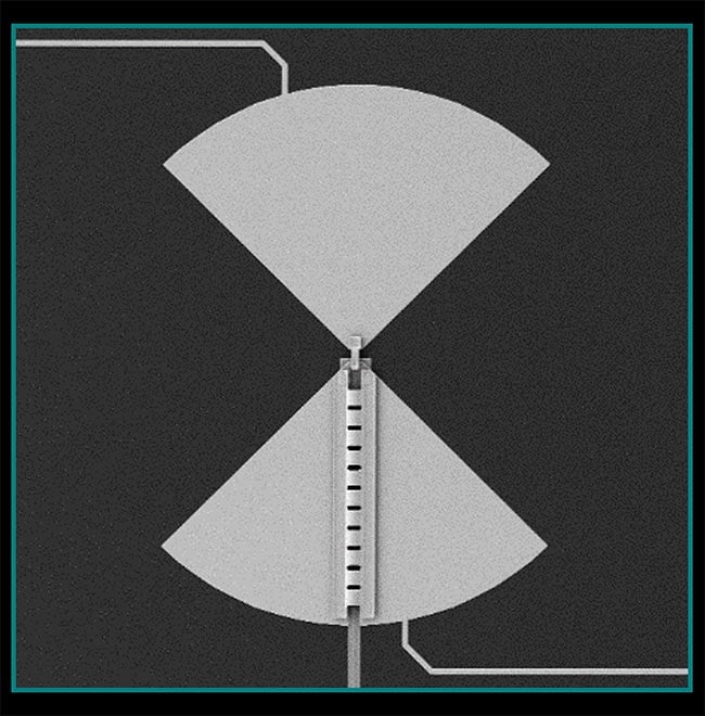
Figure 1. Terahertz source technology is enabling sophisticated deployments of terahertz radiation. This waveguide-integrated photodiode generates continuous-wave (CW) terahertz waves and uses a bow tie antenna for optimum radiation. The antenna “wings” have a width of ~500 µm. Courtesy of Fraunhofer HHI.
The integration of sources and sensors has enabled engineers to conceptualize and develop professional systems; for example, frequency-modulated continuous-wave (FMCW) spectrometers. For instance, one such system, developed by Fraunhofer Institute for Telecommunications, Heinrich-Hertz-Institute, HHI (Fraunhofer HHI), offers up to 4-THz bandwidth and up to 500-Hz measurement rates.
ToF measurement: a dominant application
Terahertz sensors have conquered many fields of application. They range from materials science and quality control to gas sensing and security applications — which nearly all of us have encountered at airports. These terahertz scanners use
radiation between 50 and 100 GHz. Though these values are not squarely in the range of terahertz radiation, the scanners take advantage of terahertz radiation
to penetrate many materials without ionization, which poses a health risk. This quality is unachievable using x-rays.
Two types of terahertz measurements are prevalent: The measurement may record a time-of-flight (ToF) signal, or a spectrum. Most often, ToF measurements use pulsed radiation, although the same information can be retrieved from the phase evolution of CW sources.
A typical application for a ToF measurement is the determination of layer thickness in automotive coatings. As shown in Figure 2, most cars are painted with several layers of color, both to achieve a shiny color as well as to protect against scratches, corrosion, and chemicals. The interfaces between the coating layers reflect part of the terahertz radiation. The resulting signal shows spikes, the temporal distance(s) of which can be converted into distances with a precision
depending on the pulse width of the terahertz pulse.
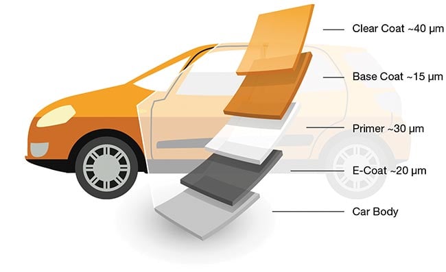
Figure 2. Cars are commonly coated with a system of protective and illustrative coatings. The multilayered approach ensures a favorable appearance and guards against scratches, corrosion, and chemicals (left). The interfaces between the coating layers reflect part of the terahertz radiation. For radiation, 10 µm corresponds to 30 fs. Courtesy of Fraunhofer HHI.
Many materials are at least partially transparent to terahertz waves. And as this radiation is nonionizing, it can be used well on humans or sensitive materials. This applies to the obvious example of airport scanners, although as mentioned, their wavelength, in the millimeter range, corresponds to the lower limit of what is defined as terahertz radiation.
A less obvious example comes from TOPTICA Photonics in a test of fast terahertz screening of pharmaceutical packaging. European legislation demands that these packages are only to be sold with patient information leaflets enclosed. Weighing the packaging usually suffices
to complete this test. However, this method may not always yield the correct “yes” or “no” answer regarding the presence of the leaflet.
In proof-of-principle measurements, TOPTICA researchers showed that fast terahertz screening detected the presence or absence of a package insert unambiguously. The method succeeded even for samples moving at >20 m/s and for boxes that overlapped in a tile-like manner.
In an additional application, terahertz sensors can be used to identify certain gases, especially in ambient settings and in trace amounts; many materials have fingerprint characteristics in the terahertz range as they do in the infrared. For this purpose, terahertz sensing is applied in a regular absorption spectroscopy setting. Figure 3 shows such a measurement system. A terahertz signal is sent through a low-pressure absorption cell with an optical path length of 5 m for the terahertz signal.
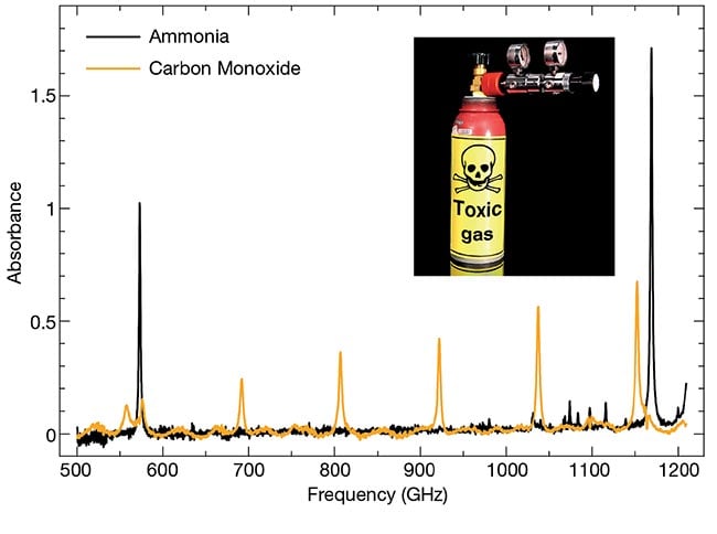
Figure 3. Absorption spectra of ammonia (black curve) and carbon monoxide (orange), measured with a continuous-wave (CW) terahertz spectroscopy system (below). Courtesy of TOPTICA Photonics.
Terahertz imaging
In many applications, requirements go beyond point measurements; for example, a body scan requires a complete image of the suspect package or person.
Accordingly, a shift is underway toward 2D- and 3D-imaging techniques using terahertz radiation, especially in industrial environments.
Beyond the obvious ToF measurements, there are several innovative approaches to measure surface properties using terahertz radiation. The German company Protemics, for example, offers systems for measuring surface conductivity based on terahertz radiation. Its system emits a terahertz pulse generated by a micron-size waveguide on a chip. Within a near-field
measurement setup, the technology enables scans of the sheet resistance on a surface.
Figure 4 shows this deployment for two types of graphene layers on silica wafers. One layer is grown directly on the surface. The other has been transferred. Protemics markets this system for measurements on solar cells, displays, transparent conductors, and flexible electronics. The maximum scan speed is 100 mm/s with a minimum scan time of 10 ms/pixel.
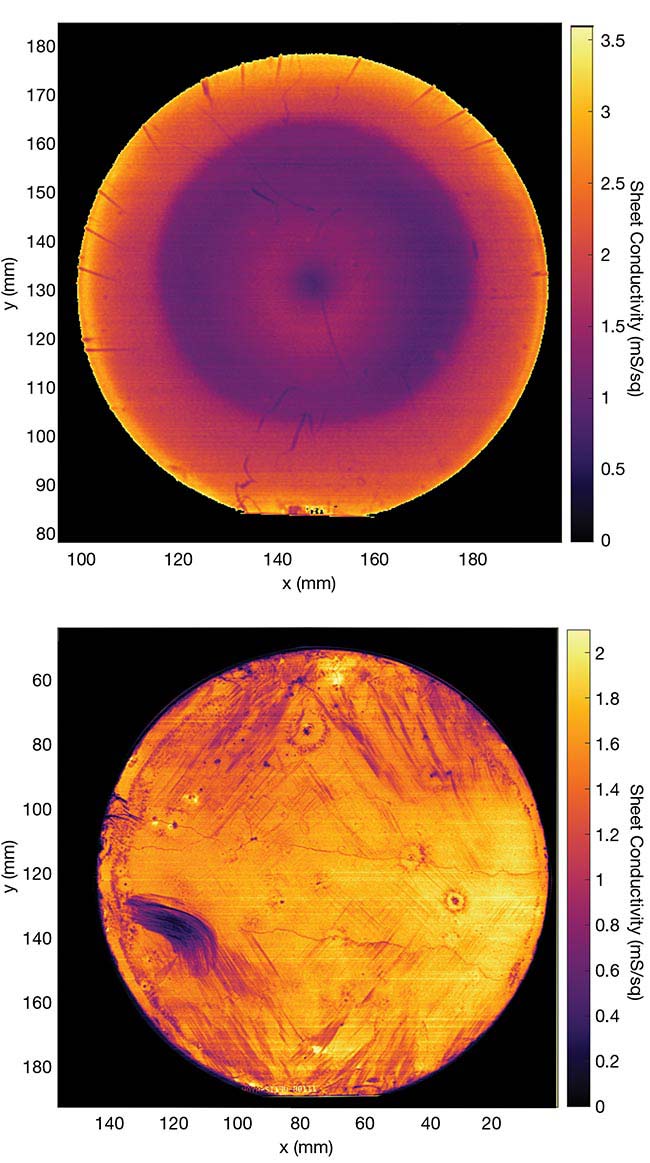
Figure 4. Sheet resistance measurement on a 4-in. sapphire wafer with directly grown graphene (top), and on a 6-in. silicon wafer with a transferred graphene layer. Courtesy of Fraunhofer HHI.
Looking ahead
Terahertz spectroscopy has left the scientific laboratory, and due to significant miniaturization, terahertz emitters and sensors presently on the market are housed in packages comparable to those of photodiodes. In addition, the advent of rugged femtosecond laser sources has supported the construction of rack-size control units.
Based on these advancements, terahertz spectroscopy is spreading into established applications, such as layer thickness measurements, as well as into new areas, such as semiconductor surface inspection. This technology is rapidly evolving toward greater integration and 2D- and 3D-imaging solutions.
Meet the authors
Lars Liebermeister has worked in the Terahertz Sensors and Systems Group at the Fraunhofer Heinrich-Hertz-Institute since 2016, becoming deputy group leader in 2019. He holds a Ph.D. in photonics from the Ludwig-Maximilians-Universität; email: [email protected].
Robert Kohlhaas has served as head of the Terahertz Group at Fraunhofer HHI since 2022, researching photonic terahertz devices and systems. He studied physics at the Technische Universität Berlin, where he also completed his Ph.D.; email: [email protected].
Andreas Thoss, Ph.D., is a laser physicist, founder of THOSS Media, and a contributing editor to Photonics Spectra. He has been
writing and editing technical texts, with a
focus on the field of photonics, for two
decades; email: [email protected].