DAEJEON, South Korea, March 30, 2017 — To increase the speed of data transfer when many microprocessors are used in parallel, a novel device has been developed that uses surface plasmons to mediate optoelectronic imaging. The on-chip plasmonic switching device consists of a 2D disordered array of nanoholes on a thin metal film that can provide multiple-input and multiple-output channels for transferring information from a photonic to an electronic platform.

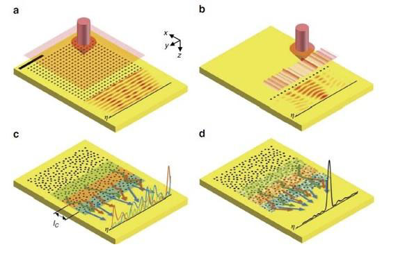
Numerical and theorectical analyses describing the performance of a 2D disordered array of nanoholes in channel transfer from far-field input to SPP output. (a) A 2D array of periodic nanoholes patterned on a metal film. (b) A 1D array of nanoholes patterned on a metal film. (c) A 2D array of disordered nanoholes patterned on a metal film. (d) The same pattern of nanoholes as (c), but the correct choice of wavefront for the illuminations at the blue, red and green rectangular areas can cause the SPPs to constructively interfere at the target point (black curve). Courtesy of IBS.
The research team, from the Institute for Basic Science (IBS), randomly arranged the nano antennas instead of periodically arranging them. The surface plasmons generated at each antenna underwent multiple scattering to minimize redundancy between the antennas. The team exploited the decorrelation effect to use individual nanoholes as independent antennas. Because each of the antennas could be used independently, the number of effective antennas increased substantially over the number that would be effective if the antennas were periodically arranged. The device demonstrated the ability to deliver more than 40 far-field incident channels simultaneously to the surface plasma polariton (SPP) channels. The use of lower loss material than gold (such as silver) could increase channel capacity even further.

Expected enhancement factor for channel number. Courtesy of IBS.
With the increased transmission channel number, the researchers implemented the simultaneous control of six SPP channels at high signal-to-noise ratios. An additional experiment involved the delivery of a 2D image embedded in far-field waves to the SPPs sampled along a 1D line, and confirmed that the nanoholes distributed across the 2D area acted as independent transmission antennas.
“We are proposing a new way to connect nanoscale microprocessors to ultra-high-speed optical communications,” said Wonshik Choi, associate director of the IBS Center for Molecular Spectroscopy and Dynamics.
Random multiple scattering by disorderly arranged nano antennas is unpredictable, and cannot be used for information transfer without taking special measures. To exploit the benefit of disordered arrangement of antennas, the team analyzed the patterns of multiple-scattered surface plasmons for various optical inputs to find an optical input signal that could send the desired signal to a specific microprocessor. A spatial light modulator was used to generate this optical input signal, allowing control of the surface plasmon.
“Using this, we proved that we can transmit signals to six different microprocessors at the same time and proved that optical images are converted into plasmons,” said Choi.
The researchers believe that their method of maximizing the deliverable far-field input channels to the plasmonic output channels could expedite the use of plasmonics in optoelectronic devices, leading to an increase in the processing speed for complex computational tasks.
The research was published in Nature Communications (doi: 10.1038/ncomms14636).