Developed for microelectromechanical systems testing, the through-transmissive-media technique has potential applications in fields from materials science to the life sciences.
Stephen Hopkins, Veeco Instruments Inc.
For decades, high-performance optical profilers have been evolving to adapt white-light interferometry to research and production applications in materials science, semiconductors, optics and the biological sciences. However, a limitation that remained largely unconquered by profiler technology was an inability to characterize through cover glass, protective packaging, environmental chamber windows or other dispersive materials. When attempting to measure through transparent layers, the resolution degraded with any increase in magnification.
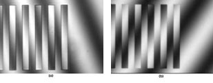
Figure 1. Images of a 20-μm-pitch standard show comparable contrast between a measurement with 3-mm cover glass taken via a 20 Michelson objective and the through-transmissive-media module (a) and measurement without cover glass imaged with a conventional objective (b).
A novel optical profiling technology that recently became commercially available enables subnanometer measurements through transmissive media at up to 40× magnification. This through-transmissive-media technique corrects for aberration, shape illumination and dispersion resulting from transparent materials above a sample. The measurements exhibit performance on a par with optical profiling measurements of materials without a covering.
The initial impetus for the development of through-transmissive-media technology was to enable optical profilers to test microelectromechanical systems (MEMS) devices in their packaged state, which typically involves a protective surface such as glass, plastic or sapphire. Featuring integrated mechanical elements, sensors, actuators and electronics on a common silicon substrate, MEMS devices are manufactured using techniques similar to the batch fabrication employed in the production of integrated circuits.
With such complexity, and facing stringent requirements on repeatability, quality control is a crucial factor in making a successful and affordable MEMS product, and it is estimated that approximately 50 to 80 percent of the total cost of MEMS production is the result of the final packaging and testing.
Because of their high speed, accuracy and flexibility, optical profilers have been widely used for measuring the surface features of unpackaged MEMS devices. The basic operation of an optical profiler is to split a beam of light exiting a single source into two beams and then to recombine them. One beam reflects from the object under test, and the other reflects from a reference mirror (Figure 2a). The beams are recombined to create fringes — bright and dark bands that represent the topography of the object.
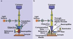
Figure 2. Schematic diagrams reveal differences between a standard interferometric optical profiler (a) and a profiler with through-transmissive-media compensation, a high-magnification objective and shaped illumination (b).
Typically, these interferometric measurements are made early in the MEMS manufacturing process. Most devices, however, perform differently once they are encased in their final packaging, which may involve vacuum, elevated-temperature or other special environments.
Low-magnification objectives capable of imaging through dispersive media with varying degrees of success have been available for several years. These methods compensate for transparent packaging material or cover glass by affixing a slice of the same material and thickness in the reference path of the interferometer.
Changing materials is cumbersome, time-consuming and sometimes even impossible. Thus, these methods lack the desired flexibility for manufacturing environments that handle materials of multiple types and thickness for the packaging of various devices.
Furthermore, as MEMS technology continues to be made smaller and even more complex, test and measurement systems require higher magnifications to resolve key features. This has been problematic for existing optical profiling technology because dispersion and aberration effects increase with magnification. Also, long-working-distance optics are required to accommodate the distance between the top of the protective layer and the surface of the MEMS device. And the objectives typically used for high magnifications do not provide adequate room to add compensation material.
These and related factors have kept optical profiling from being more useful in final-stage MEMS research and production measurement.
Magnification dilemma
There are three major issues to be resolved for the measurement of packaged MEMS with an optical profiler. First, even with matching material in the reference arm, the base image quality is poor for a 20× or higher magnification objective as a result of increased aberration from the material. Second, it is impossible to get clear interference fringes with high contrast, even with the matched dispersion from a compensator in the reference path, because of the base optical path difference, material dispersion and the diverging angle of the illumination beam. Finally, various fixed thicknesses of MEMS packaging affect image quality and fringe contrast.
Interference microscopy, which combines an interferometer and a microscope into one instrument to measure surfaces with high resolving power, uses various physical configurations to generate the interference. In a standard Michelson interferometer objective, a beamsplitter cube and a reference mirror are inserted between the objective and the tested surface. A variation of this, the Mirau objective, typically is used for midrange to higher magnifications because it minimizes aberrations from and the physical space required for the interferometric elements.
The problem is that there is no good way to add a compensation slide in the Mirau design. Although a Michelson objective has sufficient room to do so, the focus quality decreases with increased numerical aperture and varying cover media thickness, and the fringe contrast washes out.
To overcome those challenges, researchers at Veeco Instruments Inc. combined additional optics to correct for aberration and dispersion within the extra room provided by the Michelson design, and they introduced an external illuminator module (Figure 2b). The module uses an LED source and a fiber optic connector to focus a shaped beam at the sample, which provides high fringe contrast and intensity and enables the testing of samples with a transmissive cover at a system resolution of up to 40× (a 20× through-transmissive-media objective and a 2× field-of-view lens).
To verify the performance of the through-transmissive-media objective, a 20-μm-pitch standard, a fused silica mirror, and NIST-traceable 97-nm and 10-μm step-height standards were measured at 20×, uncovered, to establish a baseline. A 2× system magnification was used so that total magnification was 40×. The samples then were measured at the same magnification through 3-mm-thick cover glass, which also was used as compensation in the objective.
The experimental values for the average step height (97.3 ±0.026 nm and 9.927 ±0.005 μm), linewidth (19.836 ±0.006 μm) and roughness (0.344 ±0.003 nm) proved to be virtually equivalent between the standard objective and the compensated version, with no noticeable degradation in performance (Figure 1). Similar verifications on 2× and 10× through-transmissive-media objectives had the same positive results.
In sum, the through-transmissive-media technology solves the three limiting issues for the measurement of packaged MEMS by combining a compensating element and corrective factors with substantially collimated reference and test beams. This enables the analysis of a packaged sample surface at high magnification with the same contrast and resolution that are obtained with standard optical profiling of uncovered sample surfaces.
Commercial viability
The challenge thus became making the technology simple, affordable and flexible enough to warrant its commercial use. One of the primary engineering requirements was to take advantage of the method’s ability to measure through various thicknesses of cover material. Thought had to be given to how the introduced objectives and aberration adjustments in the objective module could be made to quickly work with a different compensation slide and its unique dispersive elements.
In the final through-transmissive-media module design, the objective module is compatible with compensating slide thicknesses in the measure-through range of 0 to 4 mm. The compensation slide is easily replaced, permitting quick measurement of samples through varying transmissive media, and the configuration of the objective module may be changed using a quick-release adapter for objectives (2×, 10× and 20×) and a fiber optic cable for the illuminator module. The illuminator contains both narrow- and broadband sources, which are software-controllable, to enable both vertical-scanning and phase-shifting interferometry. It takes only about 30 seconds to switch out the compensation material, refocus the reference mirror and obtain fringes.
The module has been employed in real-world conditions to test MEMS. At Sandia National Laboratories in Albuquerque, N.M., a packaged lateral resonator was measured through 3 mm of cover glass, with no loss of image quality (Figure 3).
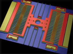
Figure 3. A false-color, 3-D map shows a lateral resonator imaged through 3-mm cover glass. Courtesy of Sandia National Laboratories.
Another static MEMS device (an RF-MEMS switch) was tested at Imec in Louvain, Belgium, showing comparable results between an uncovered MEMS device imaged at 10× (Figure 4a) and the same device after zero-level packaging using benzocyclobutene (BCB) as a sealing ring and 736-μm glass cap, imaged with a 10× through-transmissive-media objective (Figure 4b). An image of the glass/BCB interface showed an imperfect seal (Figure 4c), suggesting that the method can be used to study the sealing properties of BCB with much better resolution than conventional techniques such as scanning acoustic microscopy or x-ray imaging provide.
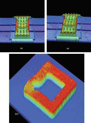
Figure 4. A false-color, 3-D analysis of a microscale switch shows the uncovered sample imaged with a 10× through-transmissive-media objective without compensation (a), after zero-level packaging using a benzocyclobutene (BCB) sealing ring and glass cap, imaged through 700-μm-thick glass using a 10× through-transmissive-media objective with compensation (b), and the glass/BCB interface using the 10× through-transmissive-media objective with compensation (c). Courtesy of Imec.
Sandia also used the system to measure devices inside small environmental chambers. The chambers have low profiles that allow them to fit under a microscope, while providing a volume within which investigators can subject devices to various pressures, temperatures and atmospheric chemistries. They also typically include a transparent window to enable observation of the sample.
An optical mirror array was imaged inside an environmental chamber, made by Linkam Scientific Instruments Ltd. of Tadworth, UK, through 170-μm-thick glass with a standard objective and a through-transmissive-media objective. The sample was exposed to temperatures of up to 150 °C to determine how elevated temperatures would affect the surface of the mirrors.
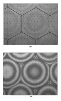
Figure 5. A micromirror array imaged through the window of an environmental chamber without compensation (a) and with compensation (b) illustrates the effects on the fringe contrast. Courtesy of Sandia National Laboratories.
Although 170 μm is fairly thin, the fringe contrast with the standard 103 objective was poor (Figure 5a). By compensating the objective with the chamber glass, however, the fringe contrast greatly improved (Figure 5b).
The data from these measurements allowed the researchers to determine how the radius of curvature, shape and roughness changed as a function of temperature (Figure 6). The same technique could be applied to samples tested in vacuum or in other environments.
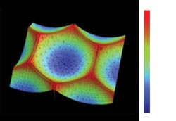
Figure 6. A 3-D analysis of a micromirror array imaged inside an environmental chamber with a through-transmissive-media objective shows how radius of curvature, shape and roughness change as a function of temperature. Courtesy of Sandia National Laboratories.
Wider application
By optimizing many factors, including dispersive compensation, coherence effects, thickness variation insensitivity and illumination, the technology improves on earlier interferometric techniques to measure surfaces underneath transmissive materials at high magnifications. Incorporating this technology, a standard optical profiler can characterize samples through transparent media up to 4 mm thick, providing in situ data on a device’s performance and material behavior under varyingenvironmental conditions.
Comparisons between standard objectives and dispersion-compensated objectives, as well as on initial MEMS application samples, show that the through-transmissive-media method offers results that equal unpackaged MEMS measurements performed with a standard profiler. With the commercial production of this technology, optical profiling can measure critical MEMS features throughout the development and manufacturing process, including final tests in transparent packaging.
Perhaps even more exciting is that this technology opens doors for a vast array of existing and emerging applications in fields from materials research to the life sciences. With the ability to characterize through transmissive media, this module allows researchers and manufacturers to image through environmental chambers, liquids and other dispersive materials with all the accuracy, speed and flexibility for which optical profiling is known.
Meet the author
Stephen Hopkins is a marketing communications specialist at Veeco Instruments Inc. in Tucson, Ariz.; e-mail: [email protected].