ALBUQUERQUE, N.M., March 28, 2017 — Materials that are more efficient than metals and that feature wider bandgap measures than silicon are being developed for possible use in optical metamaterial applications. All-dielectric materials using III-V semiconductors could be used to develop metamaterials that are efficient, resistant to energy loss and able to operate in the IR range.

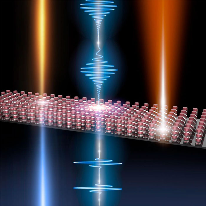
This three-resonator-thick III-V metasurface of cylindrical resonators illustrates three possible uses: The left light beam changes color as it passes through the metasurfaces, signifying that nonlinear harmonic generation is taking place, which converts the light beam to a shorter wavelength. The blue trace in the middle shows a train of pulses passing through the surface. As they pass, the pulse width decreases due to pulse compression, which requires that the phase of the transmitted optical wave vary with the wavelength. The multilayer metasurfaces are able to achieve the correct phase variation -- something not possible with single layer metasurfaces. The beam on the right signifies that these metasurfaces can act as efficient emitters of light. Courtesy of Sandia National Laboratories.
Artificial atoms, known as resonators, form the guts of the metamaterial. Created under the supervision of Sheng Liu, a researcher at Sandia National Laboratories, the meta-atoms are a few hundred nm in diameter and made of many actual atoms. Liu oxidized the atom groupings around their perimeters to create layered coatings with a low index of refraction.
The oxidized, low-index surface surrounded the high-index core “like in wintertime, you have a coat surrounding you,” Liu said. “To confine light, you need a high refractive-index contrast.”
Controlled oxidation was achieved by putting the III-V materials in a hot oven and flowing water vapor over the sample. The meta-atoms were sculpted in place during a lithographic process that permitted the researchers to make any pattern they chose for the placement of the metamaterial components.

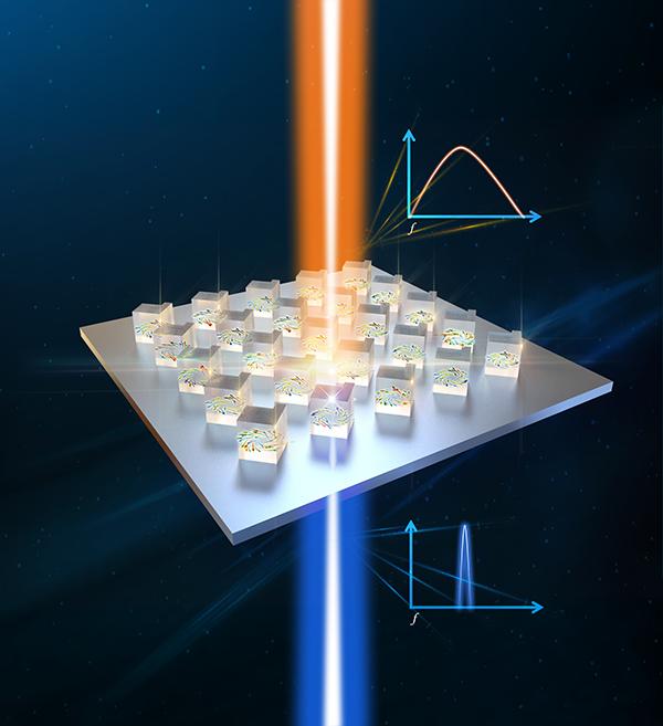
The broken-symmetry metasurface of cuboid resonators shows a spectrally broad incoming light wave. (The graph on top shows a broad spectrum.) After passing through the metasurface, the beam becomes spectrally narrow due to the sharp resonances of the broken symmetry metasurface. (The graph on the bottom shows a narrow spectrum.) The swirling pattern of arrows represents the electric field distribution of light trapped in the resonators. Courtesy of Sandia National Laboratories.
The researchers utilized symmetry breaking of highly symmetric resonator geometries, such as cubes, to induce couplings between the otherwise orthogonal resonator modes. They designed perturbations that coupled “bright” dipole modes to “dark” dipole modes whose radiative decay was suppressed by local field effects in the array.
The researchers unraveled the Fano resonance behavior through numerical simulations of a germanium resonator-based metasurface that achieved a quality factor of ∼1300 at ∼10.8 μm. They conducted two experimental demonstrations operating in the NIR (∼1 μm): a silicon-based implementation that achieved a quality factor of ∼350 and a gallium arsenide-based structure that achieved a quality factor of ∼600.

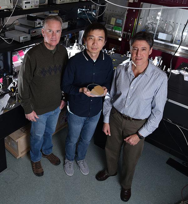
Sandia National Laboratories researchers Igal Brener, right, Sheng Liu, center, and Mike Sinclair stand in the laboratory where work was done to create metamaterials on substrates. Liu presents one version here. Courtesy of Sandia National Laboratories.
The research team describes their approach as scalable from the NIR to radio frequencies. They believe that combining high quality factor, high field enhancement resonances with nonlinear and active/gain materials such as gallium arsenide could lead to novel classes of active optical devices, such as ultra-thin lenses and ultra-efficient cell phone antennas; devices to bend light to keep satellites cooler; or to make photovoltaics more energy absorbent.
“We feel we've created a pretty flexible platform for a lot of different kinds of devices,” researcher Mike Sinclair said.
Three patents on aspects of the work have been submitted.
The research was published in ACS Photonics (doi: 10.1021/acsphotonics.6b00556).