Size, power, contrast and color space advantages make OLED microdisplays a perfect fit for near-eye applications. Advances in subpixel patterning and the development of stacked OLEDs promise to extend color space and battery life.
UWE VOGEL, FRAUNHOFER INSTITUTE FOR ORGANIC ELECTRONICS, ELECTRON BEAM AND PLASMA TECHNOLOGY FEP
Mobile personal electronics and wearables have become immensely popular around the globe, and this has given rise to a new dilemma. Screen content has grown, mainly from multimedia applications, resulting in increased display pixel count. The initial black and white character displays in early mobile phones have evolved into full-HD (FHD), full-color video displays and beyond. Even the screen diagonals have become larger: There is only a single smartphone product on the market featuring FHD active-matrix organic light-emitting diodes (AM-OLEDs) at <5 in. (Samsung Galaxy S4), but many at larger screen formats. Besides the technical issues of achieving high pixel density, most mobile display screen sizes are bigger than 5 in., and, depending on the geographic region, even greater than 7 in.
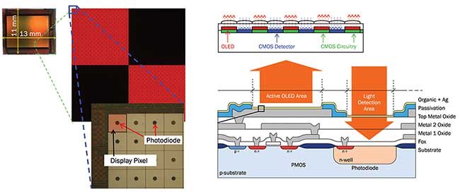
General setup of a bidirectional OLED microdisplay (left). Courtesy of Fraunhofer FEP.
However, content will continue to increase, and will continue to do so, especially with upcoming virtual- and augmented-reality applications. Yet users generally prefer to keep their smartphones “mobile” and thus need to limit the size of the device, hence the display screen size. Fortunately, set manufacturers have managed to keep the device size very close to the display size, and do not require much extra space beyond it.
There are two general ways to address the balancing act of mobile screen content versus size: The first is to create a physically larger screen size at a reduced form-factor. This would be a move away from rigid planar screens; for example, they could be made rollable, to fit into smaller spaces.
Another option is to move from direct view toward projection, by generating a larger screen perception toward the user by either real or virtual optical magnification. The latter one is the opportunity for microdisplays in general since, due to their unprecedented pixel density, they are able to generate high-resolution virtual images with a large viewing angle at a very small device footprint.
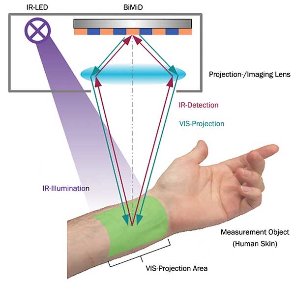
Principle setup of veins viewer based on bidirectional OLED microdisplay. Constanze Großmann et al. (2013) A novel concept of a veins viewer based on bidirectional OLED microdisplay. SID Symposium Digest of Technical Papers, Vol. 44, Issue 1, pp. 142-145. Courtesy of Fraunhofer IOF.
All microdisplay technologies on the market comprise an image-creating pixel modulation, but only the emissive ones (for example, OLED and LED) feature the image and light source in a single device, and therefore do not require an external light source. This minimizes system size and power consumption, while providing exceptional contrast and color space. Organic light-emitting diodes (OLEDs) are made from ultra-thin organic semiconducting layers, which light up when they are connected to voltage (charge carriers become injected and luminance mainly is proportional to the forward current). The major layers comprise several organic materials in sequence (for example, charge transport, blocking and emission layers — each with a thickness of several nanometers), which are inserted between an anode and a cathode. OLED microdisplays cover the major portion of emissive microdisplays on the market today as they are well-suited for extremely small form-factor and low-power consuming optical engines. They are the first choice for mobile.
Near-to-eye applications growing
The growing market for wearable devices requires a high number of small and lightweight displays for different applications in sports, medicine or at work. The global market for microdisplays expanded in the 1990s, mainly due to rising demand for projection applications, specifically front projectors and rear-projection TV (RPTV). Whereas RPTV significantly declined after 2005, other applications have arrived, mainly in near-to-eye (NTE) displays.
Due to the size, power, contrast and color-space advantages, NTE applications represent the largest opportunity for OLED microdisplays. This relates to both personal viewers (PV) and electronic viewfinders (EVF). As of today, there are three main markets for near-eye OLED micro-displays. The consumer market encompasses video and virtual-reality (VR) glasses and EVF; industrial covers augmented-reality (AR) smart glasses for logistics; defense market targets AR helmets for pilots.
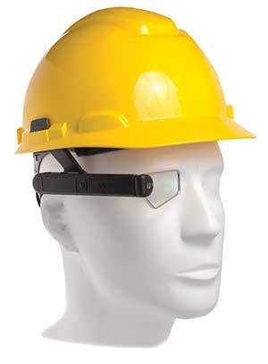
Vuzix M3000 Smart Glasses. Courtesy of Vuzix.
PV are either see-through data glasses used for mixed- and augmented reality (AR) applications, or non-see-through/immersive video glasses used for entertainment or virtual reality (VR) applications in gaming, training or entertainment. Due to their emissive nature OLED microdisplays are specifically suited for see-through/AR smart glasses, since they prevent a virtual gray-shaded monitor-like perception inside the user’s field of view, which is caused by the insufficient backlight suppression of non-emissive microdisplays.
Although other products had been on the market for quite some time, Google garnered global attention with the launch of Google Glass in 2012, ostensibly aimed at the consumer market. Instead, it was shipped to individual customers/developers in limited quantities and has been used in a few niche professional applications, including fabrication logistics at Volkswagen in Wolfsburg, Germany.1
Today, suppliers of personal viewers include Vuzix, Google, Epson, Brother, Sony, Zeiss, NVIS Inc., eMagin and Lumus Ltd., with others including Meta, Atheer, Optinvent and Samsung Electronics. There are also personal viewers, mainly for fully immersive VR applications, that make use of midsize TFT displays (which are not microdisplays), Oculus Rift or Zeiss VR One.
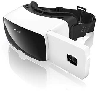
Zeiss VR ONE video glasses. Courtesy of Zeiss.
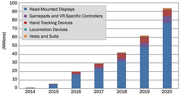
The market is expected to grow significantly in PV applications, with major expected growth for see-through data glasses. The market analysis firm Tractica estimates that smart augmented-reality glass shipments will surpass 12 million units between 2015 and 2020, while more than 200 million virtual reality head-mounted displays will be sold by 20202. Consumer and enterprise segments will both drive sector growth, with additional sizable markets for industrial and sports applications.
Electronic viewfinders in cameras
In the past few years several leading camera makers including Sony, Panasonic, Olympus and Fujifilm released cameras — mostly high-end models that adopt OLED microdisplays for the EVF. In 2012 microdisplay unit shipments for electronic viewfinders were 4 million, with 7 million in 2013, according to a report from Insight Media in 20133. The market should continue to grow significantly, with an expected shift of EVFs from primarily high-end cameras toward midrange consumer devices. There is also a market in EVF for digital video cameras and camcorders; however, this is expected to decline driven by a shrinking camcorder market and the use of direct view panels in high-end viewfinders.
Micro-projection in sight
Projection is still the major application of microdisplays. Due to limited luminance and luminous flux capabilities of OLED, the use of OLED microdisplays for front-projection has been limited. However, in 2010 the European Commission-funded HYPOLED project demonstrated OLED microdisplays in micro-projection, though full-color projection had only been feasible using a three-panel approach comprising three monochrome subpanels (R, G, B) and optical color-combining. Red and green monochrome micro-projectors worked quite well at limited luminous flux, but displays had to be driven at around 10000 nits (a nit is a unit of luminance equivalent to one candela per square meter). This significantly affected OLED lifetime.
Alternative OLED microdisplay projection applications, mainly in combination with Fraunhofer FEP’s bidirectional OLED microdisplay approach, have been presented by Fraunhofer IOF. A bidirectional OLED microdisplay refers to a device capable of image display and image sensor/acquisition by the same chip and in parallel.4

The forearm to be imaged (a); the detected IR image of the forearm at 890 nm (b); the projected image of (b) at 622 nm onto a screen with a red monochrome bidirectional OLED microdisplay (c); the projected image onto the human skin (d). The image is congruent with the real vein structure. Courtesy of Fraunhofer IOF.
OLED-on-silicon
The prominent emissive microdisplay technology on the market is OLED-on-silicon. A single-crystalline silicon CMOS chip provides the active-matrix circuitry to address and drive the millions of individual pixels. Since the silicon substrate itself is intransparent in the visible spectrum, a top-emission OLED setup is required. Today’s relevant commercial players in the OLED microdisplay market are Microoled in France, eMagin in the U.S., Sony in Japan and Olightek in China.
It’s worth noting that emissive microdisplay technology might be most suitable for so-called bidirectional microdisplay techniques, which combine both image display and image acquisition in a single chip. That’s mainly due to the fact that there is no intrinsic saturation of photodetectors embedded inside the microdisplay backplane caused by the external illumination of “modulating” displays, in contrast to the top-emission, though optical cross-talk inside the emissive microdisplay device should be factored in. Image sensor elements, for example, pn-junction CMOS photodiodes, are arranged in a fixed matrix/pixel pattern correlated to the image display pixel matrix/pattern. In a common case, both arrays have become intersected to each other; one photodetector pixel per one display pixel. Other design arrangements are feasible and should be adapted to the application. Moreover, optical crosstalk effects can be limited or avoided by design, driving scheme and technological means.
LED microdisplays
The term “microLED” refers to a variety of approaches that combine III/V-based inorganic LEDs with a silicon backplane, either monolithically or hybrid. Examples come from several startups and universities, including Ostendo, InfiniLED, LuxVue, Lumiode or the University of Strathclyde/the University of Edinburgh5.
Due to recent promising activities of III/V LED or RF/power component manufacturers to transfer III/V processes onto silicon-compatible 8-in. equipment for cost reasons, monolithic silicon-III/V hetero-integration — GaN-on-Silicon, for example — could become a competitive technology for emissive microdisplays in about 10 years. Cost may be comparable to OLED-on-silicon over the long run, but some characteristics such as lifetime, high-temperature performance, spectral width and switching speed, could prove superior.
Technical challenges of OLED microdisplays
Luminance and lifetime are two critical performance parameters for OLED microdisplays, specifically under high-temperature conditions. For cost reasons, achieving low-pixel pitch is important, since it directly translates into die size and chip cost. For immersive environments such as non-see-through or EVF and NTE applications, luminance up to 500 cd/m2 and lifetime >10,000 hours are usually sufficient, whereas current see-through optics and consideration of sunlight conditions easily demand >5,000 cd/m2 of luminance and beyond, regularly combined with elevated temperature operation. The challenge at high luminance is to supply and modulate the forward voltage at dynamic range levels of 2V up to 7 V toward each OLED pixel; this requires integrated driving transistors able to withstand voltage swing of 5 V or more. That’s a high voltage for advanced mixed-signal CMOS processes at minimum feature sizes, which are usually referenced by minimum transistor channel length, for example, in the range of 0.25 to 0.11 µm at core voltages of about 1.2 to 2.5 V. Such high-voltage transistors require more die area, whereas smaller feature size CMOS processes typically provide even fewer options for HV devices, i.e., shrinking pixel cell size remains limited.
The OLED layers need to be protected against oxygen and water vapor. The thin-film encapsulation is typically realized via Vitex (monomer and AlOx-multilayer), atomic layer deposition (ALD) combined with an organic/inorganic layer as well as approaches of purely inorganic encapsulation. There are several suppliers on the market that offer encapsulation approaches, but Vitex and ALD are the only industry-proven encapsulation methods for OLED microdisplays so far.
Overview of microdisplay technology and selected commercial suppliers. Courtesy of Tractica.
The deposition of a color filter directly on the thin-film encapsulation of the OLED is a highly critical process due to the direct contact of the encapsulation with solvents of the filter and high temperatures during baking. eMagin is known to use this approach, which requires a temperature-stable OLED stack (a white OLED combined with red, green and blue filters) to survive the color filter baking process. The lamination of an additional color filter wafer is the second approach to produce monochrome colors by white OLEDs.
Fraunhofer FEP has applied the latter approach by using 200-mm wafers with an externally supplied color filter wafer. The process of laminating the CMOS/OLED wafer with a color filter wafer is challenging due to the need for high wafer alignment accuracy and internal forces between both wafers with an adhesive layer in between. The high alignment accuracy is needed due to pixel gaps of <1 µm; therefore CMOS and color filter wafer must be aligned across the whole wafer with an accuracy of better than 1 µm as well. This is challenging due to different lithography and alignment processes of the CMOS and color filter supplier and the laminating process itself, which requires stable wafer-to-wafer positioning during adhesive curing. Both color filter approaches have been used in production and achieve sufficient yield to compete against each other, whereas the latter one might provide limits for pixel-shrinking significantly below 5 µm.
Subpixel patterning
To address the challenges of high luminance operation, improvements are required in the current color generation approach by white OLED emission and absorption-filter color separation. To overcome this luminance/power-inefficient approach, monochrome subpixels featuring individual spectral emitters in red, green and blue could be a better alternative. That would directly benefit current and power efficiency, thus lifetime, and color space. For direct-view active-matrix organic light-emitting diode (AMOLED) displays, such an approach has been in large volume production at Samsung Display by shadow-masking or “fine metal masking,” but those and other patterning approaches currently exhibit a lower feature size limit at about 50 µm. The OLED microdisplay feature sizes in the range of 5 µm or below have not been shown in a productive micropatterning process so far.
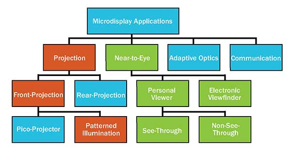
Microdisplay applications (green: OLED microdisplays established; turquoise: future markets for OLED microdisplays). Courtesy of Fraunhofer FEP.
Unfortunately, the high-resolution photolithography commonly adopted in microelectronics cannot be applied to OLED easily, since their photochemistry materials are going to affect the organic semiconductor materials due to their hydrophilic behavior. There are potential options to overcome this issue; for example, one way involves the effect of chemical orthogonality to a specifically adapted photochemistry for organic semiconductors6. Alternative approaches could involve micro-shadow-masking, flash mask transfer lithography or electron beam patterning, the latter one to be presented by Fraunhofer FEP at SID Display Week 2016 in May. Yet any of those have to prove manufacturing feasibility for micropatterning for OLED microdisplays.
Future forward: OLED-on-silicon
There is a trend toward high-brightness, and improved current and power efficiency, as can be seen in the development of stacked OLED devices. This will be accompanied by a monochrome subpixel micropatterning approach, which will extend color space and battery life for mobile applications. That’s always an important driving force, which may lead to new low-power microdisplay architectures. Specifically the bidirectional OLED microdisplay feature provides great opportunity for OLED microdisplay applications well beyond near-to-eye, for example, in optical inspection and optoelectronic sensors.
References
1. http://www.techtimes.com/articles/110662/20151125/volkswagen-employees-appear-using-google-glass-factory.htm; https://www.tractica.com/newsroom/press-releases/smart-augmented-reality-glasses-shipments-to-surpass-12-million-units-between-2015-and-2020.
2. https://www.tractica.com/newsroom/press-releases/more-than-200-million-virtual-reality-head-mounted-displays-to-be-sold-by-2020.
3. Insight Media (2013). High-level microdisplay forecast of selected markets (December).
4. S. Riehemann et al. (2009). Ultra small OLED pico projector. Opt Photon, Vol. 4, pp. 34-36, ISSN 1863-1460; C. Großmann
et al. (2013). Novel concept of a veins viewer based on bidirectional OLED microdisplay. SID International Symposium, Vancouver, Canada.
5 J. Herrnsdorf et al. (2015). Active-matrix GaN micro light-emitting diode display with unprecedented brightness. IEEE Transactions on Electron Devices, Vol. 62, No. 6, June.
6. S. Krotkus et al. (2015). Influence of bilayer resist processing on p-i-n OLEDs: towards multicolor photolithographic structuring of organic displays. Proc SPIE, Vol. 9360, Organic Photonic Materials and Devices XVII, 93600W (March 16).
Meet the author
Uwe Vogel leads the Microdisplays and Sensors division at the Fraunhofer Institute for Organic Electronics, Electron Beam and Plasma Technology FEP, where he also serves as deputy director. Fraunhofer FEP’s general mission is application-specific R&D based on customer orders. The institute is working on OLED micro-displays, focusing on component design (including backplane IC design) and related technology and manufacturing development, as well as system integration and application; email: [email protected].
What Makes a Microdisplay a Microdisplay?
A microdisplay usually comprises the following features:
• physically very small device (screen diagonal usually <1 in., sometimes up to 1.5 in.), requiring magnifying optics to perceive enlarged image view

Microdisplay examples. Courtesy of Fraunhofer FEP.
• high information content (TV quality); according to the tiny screen size that usually translates into pixel densities >1000 ppi, or pixel pitch <25 µm (typically about 5 µm)
• active-matrix backplane (often single-crystalline silicone CMOS)
• low power consumption
In general microdisplay technology can be divided into four major categories. Three of them — emissive, reflective and transmissive — can be integrated together with a pixelated active-matrix backplane as introduced above. However, scanning microdisplays are based on high-speed deflection by a single-beam scanner. With the exception of emissive, all other technologies are modulating, meaning they require external light sources.