Higher throughputs, wider fields, and lower temperatures are broadening microscopy’s industrial applications in the infrared, ultraviolet, and terahertz ranges.
JAMES SCHLETT, CONTRIBUTING EDITOR
To produce faux marble kitchen countertops, a manufacturer places a piece of solarized polypropylene — a thermoplastic polymer material — on top of white stone. To ensure that a successful bond is created, the stone must contact the nonsolarized side of the polypropylene.
The challenge: The visible eye cannot differentiate which side is which.
Infrared and ultraviolet
imaging are extending
beyond the biomedical
and chemical settings in
which they are strongly
established. Courtesy of www.iStock.com/Pongchart.
To make this distinction, the manufacturer in a recent use case used Shimadzu Scientific Instruments’ infrared microscopy solution to determine where oxidation had occurred. Oxidation is an indication of the solarization and is therefore a useful gauge for the manufacturer.
The manufacture of faux marble countertops is one of the nontraditional — but growing —industrial applications for nonvisible microscopy, in which uses of infrared (IR), ultraviolet (UV), and terahertz wavelengths are each finding expanded adoption. Many of these applications and use cases require additional components and instrumentation that are themselves emerging. The prevalence of other applications can be attributed to the growing demand to perform functions in support of sophisticated technology areas, ranging from quantum science (computing) to materials research (semiconductor manufacturing).
Fourier transform
Certain nonvisible microscopy imaging modalities provide established options for end users in many fields, including those in the life sciences. Particle analysis, for example, is a common application in biomedical and biology research. Although industrial examples are less widespread, functions in industrial settings also commonly require particle and failure analyses, which can be performed using IR, UV, and terahertz imaging.
In the aforementioned case of the faux marble countertop, the IR microscope connects to a Fourier transform infrared (FTIR) spectrophotometer. “The IR microscope is needed for this [application] due to the spatial information that solves the customer’s problem,” said Gilbert Vial, Shimadzu Scientific Instruments’ molecular spectroscopy product manager. “An FTIR spectrometer would be able to measure the polypropylene, but you need a microscope to provide the spatial information.”
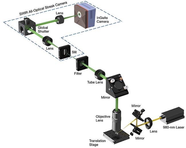
A shortwave infrared (SWIR) photoluminescence
lifetime imaging microscopy system using an
all-optical streak camera system (PLIMASC, next image) comprises many well-known
and widely used components.
InGaAs: indium gallium arsenide. Courtesy of Institut national de la recherche scientifique.
This capacity for spatial analysis is increasing IR microscopy’s use in the semiconductor, battery manufacturing, and automotive industries. With battery analysis, for example, manufacturers must determine how evenly the chemicals are spread throughout an entire space of the battery, because variations to the distribution influence the battery’s efficiency. “The IR microscope has the ability, with most manufacturers, to stitch together multiple measurement points, which allow a chemical change to be tracked over a surface. Performing this type of measurement on a sample can show how widespread the contamination is, and it can potentially show if there’s a way to salvage the product or if the entire piece needs to be discarded,” Vial said.
Kitchen countertop production is obviously not required at the volumes or scales that are demanded by semiconductors and pharmaceuticals; in these fields, FTIR microscopes are used in higher throughput applications. And for such high-throughput functions, the instruments may incorporate quantum cascade laser (QCL) sources and wide-field cameras. Classical Fourier transform relies on a thermal IR source and enables broadband IR spectroscopy, though the amount of light intensity limits its microscopic applications. The integration of QCL sources in FTIR microscopes dramatically increases light intensity. In combination with wide-field camera detectors, large areas can be illuminated and imaging measurements can be conducted at unprecedented speeds, according to Hans-Christian Koch, Bruker Switzerland’s microscopy manager.
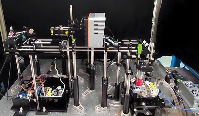
A shortwave infrared (SWIR) photoluminescence
lifetime imaging microscopy system using an
all-optical streak camera system. Courtesy of Institut national de la recherche scientifique.
An IR microscope solution from Bruker combines Fourier transform and QCL technology in a single device. “Using QCL technology, measurement speeds can be dramatically increased. For many applications, such as pharmaceutical tablet imaging or particle screening, this is a game changer,” Koch said. Additional applications for this FTIR microscopy augmented by QCLs include the analysis of the amounts of silk, cotton, and wool fibers in tissue fabric, as well as the quality control of adhesive sealing used for tea bags, to prevent them from disassembling in a cup.
Bruker’s combination of FTIR microscopy with QCL sources supports a trio of measure modes: transmission, reflectance, and attenuated total reflectance (ATR). While high-throughput capabilities may not be a top priority for all materials analysis, or for all testing laboratories that serve small-batch research applications, the ability to combine FTIR microscopy with microscope ATR offers distinct advantages. Covalent Metrology Services of Sunnyvale, Calif., has combined FTIR microscopy with microscope ATR to identify the source of small foreign particles in packaged medical devices. “This enabled the customer to isolate the elements of the manufacturing process that were introducing the particles and [to] fix them,” said Xiang Li, an engineer with Covalent Metrology. This resulted in significant savings in both in time and cost, Li said.
Failure analysis involving small particle contamination is a fast-growing application for FTIR microscopy services. Still, particles sized <100 µm are difficult to identify, as are inorganic materials with little IR absorption or nonspecific bands. The submicron size of nanoplastics, for example, would traditionally place their analysis outside the scope of IR microscopy’s capabilities.
Shimadzu is addressing the bottleneck with an FTIR microscope that can be used to obtain measurements as small as 10- × 10-µm spots, using its 15× aperture and Raman objectives that enable measurements of 3-µm spots on samples. This aperture supports the focus on small locations. Traditional FTIR benchtop systems require larger samples, close to 3 to 5 mm.
Additional limiting factors for FTIR microscopy include the slowness of mapping and low resolution, when compared with visible light optical microscopy, confocal Raman, and electron microscopy. According to Li, full-field detectors could support a viable solution, because these components enable faster mapping. And users can also improve resolutions with nano-IR, optical photothermal infrared spectroscopy, and atomic force microscope-IR spectroscopy, Li said.
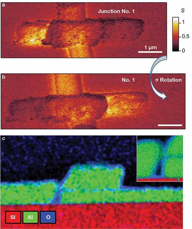
This terahertz scanning near-field optical
microscope (SNOM) image of representative
terahertz near-field images of nano-dipole fields
across Josephson junction structures indicates
a connectivity issue by showing electrical field
concentration and asymmetry. See Reference 3.
Al: aluminum; O: oxide; s: scattering amplitude;
Si: silicon. Courtesy of Ames National Laboratory.
In addition to QCL sources and wide-field imagers, systems designers are also incorporating AI and/or machine learning elements with FTIR microscopy. Often, this enhancement is introduced to customize post-processing results in FTIR microscopy. Vial cited the example of AI automatically producing a report on microplastics that details which microplastics are present in samples and quantifying them.
But AI’s confidence metrics are much more complex than those in conventional systems, for which the common library matching confidence metric is the overlap of sample and reference spectra as calculated with an inner product, Li said.
“Ultimately, to assess accuracy, what we would want to know is the rate of true positive matches, false positives, true negatives, and false negatives, and the efficacy of confidence or matching metrics in each of those scenarios,” Li said.
Advancing SWIR use cases
Anti-counterfeiting for high-security and luxury items is another application for IR microscopy. This application has commanded increased attention from institutions that handle and process these items as well as solution providers and members of the R&D community.
At the Institut national de la recherche scientifique (INRS) in Québec City, researchers developed a shortwave infrared (SWIR) imaging technique capable of capturing the photoluminescence lifetimes of rare-earth doped nanoparticles at the microsecond timescale. The technique combines wide-field SWIR microscopy and a SWIR all-optical streak camera. It uses a 980-nm pulsed laser to excite rare-earth-doped nanoparticles and detect the SWIR emission.
Jinyang Liang, an INRS associate professor, said that the developed camera solution, called SWIR photoluminescence lifetime imaging microscopy using an all-optical streak camera (SWIR-PLIMASC), could be used by instrumentation companies for fast, efficient, and affordable lifetime mapping for general purpose material characterization. It could also be used for the analysis of a material’s dynamic optical properties or structural changes, and the energy transfer process between two materials.
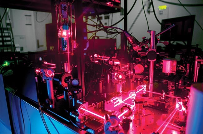
Ames National Laboratory scientists’ terahertz
scanning near-field optical microscope (SNOM)
enables measurements of frequency-dependent
dielectric and conductivity responses, with
sub-20-nm resolution and 100-fs time resolution
at 0.1 to 3 THz frequency, operating at 1.8 K
and under a magnetic field of 5 T. Courtesy of Ames National Laboratory.
The anti-counterfeiting potential that the solution offers builds on that of traditional IR-based solutions. Traditionally, IR sensors have been used to detect the spectral range emissions of rare-earth-doped nanoparticles, which are easy to counterfeit. In contrast, the developed method focuses not only on the “invisible” emission but also on the signature extracted from the measurement of transient photoluminescence intensity decay.
Illuminating the ultraviolet
Manufacturers in the semiconductor industry use UV spectroscopy for mapping devices and wafers to capture latent defects and optimize process control. This application is increasingly important with the proliferation of silicon carbide and gallium nitride devices. UV spectroscopy is used to study the layers of heterostructures for high-power devices in electric vehicles (EVs) and EV chargers as well as high-frequency devices for the 5G network, according to Rick Lytel, CEO of Klar Scientific in Pullman, Wash.
Klar has developed a spectroscopic mapping microscope that performs deep-UV (DUV) scanning to capture features in nearly every layer of a heterostructure. It is based on Klar’s confocal mapping microscopy solution that was developed for visible and near-infrared (NIR) photoluminescence applications. Early adopters of the technology focused on ultrawide bandgap materials, such as the semiconductor material gallium oxide. Subsequent uses of the instrument have involved making photoluminescence scans of regions of interest, followed by making Raman scans of specific subregions to reveal interesting features and anomalies.
The scanning method is multimodal, and for its solution, Klar uses modular optical plug-and-play kits to enable a rapid switchover from photoluminescence to Raman, or to another photoluminescence wavelength. “One client combined the Klar maps with information gleaned from scanning electron microscopy to overlay the maps and identify the source of material damage,” Lytel said.
Capturing mapping is still a challenge in using UV solutions for failure analysis. High-resolution UV mapping over portions of wafers is achievable with Klar’s system, though high-resolution maps for entire wafers and deeper-UV excitations are more challenging to achieve, Lytel said.
A current trend involves UV light sources beyond the traditional UV LEDs enhancing microspectroscopy in the DUV and NIR ranges. CRAIC Technologies, of San Dimas, Calif., has introduced an advanced illumination system from 200 to 2500 nm for both reflectance and transmission microspectroscopy and imaging. According to company president Paul Martin, one interesting application for the company’s microspectrometers is the characterization of nanostructures for which photon interactions are based on structural rather than chemical properties. One study involved metallic nanostructures with potential applications for color displays, data storage, and anti-counterfeiting technologies1. Another involved plasmonic metasurfaces with potential for use in digital displays and color printing2.
Terahertz in the quantum realm
In the high-throughput screening of quantum circuit components, terahertz microscopy is proving to be essential, as the method is operational at very low cryogenic temperatures. In partnership with the U.S. Department of Energy’s Superconducting Quantum Materials and Systems Center, scientists at Ames National Laboratory developed a terahertz scanning near-field optical microscope (SNOM) that measures frequency-dependent dielectric and conductivity responses. The microscope achieves sub-20-nm resolution and 100-fs time resolution at 0.1 to 3 THz frequency, operating at 1.8 K and under a magnetic field of 5 T. It can operate at sub-liquid helium temperatures and under a high magnetic field.
“There is no commercial SNOM instrument in the market operated at liquid helium temperature,” said Jigang Wang, an Ames Lab scientist and professor of physics and astronomy at Iowa State University.
Quantum computers process information at speeds faster than conventional computers because qubits can simultaneously exist as 0 and 1 quantum states, whereas bits can only exist as one or the other. The ability of qubits to exist in their quantum state is enabled through the Josephson junction, which controls the supercurrent flow through the circuit. This flow must be at cryogenic temperatures and remain uniform and non-dissipative.
Using the cryogenic terahertz microscope, Ames researchers discovered a defective boundary in the Josephson junction that caused conductivity disruptions and impeded quantum computation-dependent long coherences times. “By taking advantage of single- [and] few-cycle terahertz pulses, terahertz SNOM provides a noninvasive and nearly contactless way to probe the low-frequency conductivity of materials at the nanoscale and with sub-picosecond temporal resolution simultaneously,” Wang said.
“In comparison to IR microscopy, the low-frequency terahertz region is ideal for assessing the fundamental low-energy conductivity and resonance toward zero frequency associated with diverse collective modes in exotic topological states and superconductivity in condensed-matter systems.”
References
1. X.M. Goh et al. (2014). Three-dimensional plasmonic stereoscopic prints in full colour. Nat Commun, Vol. 5, No. 5361.
2. M. Song et al. (2023). Versatile full-colour nanopainting enabled by a pixelated plasmonic metasurface. Nat Nanotechnol, Vol. 18, No. 1, pp. 71-78.
3. R.H.J. Kim et al. (2023). Visualizing heterogeneous dipole fields by terahertz light coupling in individual nano-junctions. Commun Phys, Vol. 6, No. 147.