Behnam Rashidian and Eric Fox, Teledyne Dalsa
In the CMOS imaging device design process, some trade-offs are related to the physics of operating the device; others are due to practical non-idealities in the implementation of the design. To come up with an optimal CMOS imaging device design, all of these factors should be considered.
Over the past 10 years, CMOS imaging technology has been increasingly adopted by OEMs in the machine vision industry, although progress has required considerable time and investment. Integrated circuit design is always a process of optimizing trade-offs between limiters, but innovations in design and improvements in fabrication technology have allowed designers to overcome many traditional practical implementation issues and deliver products with performance that is truly compelling for machine vision applications.
Future generations of CMOS technology will continue to enhance the performance of imaging devices. Now users can benefit from high-resolution, high-speed imaging devices that provide image quality that exceeds application requirements. Future generations of CMOS technology will defy today’s limits with unprecedented combinations of imaging device attributes.

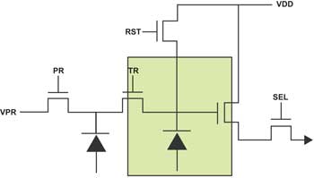
Teledyne Dalsa’s 5T global shutter CMOS pixel, introduced in 1999.
Designing the most suitable camera for a specific machine vision application requires a delicate balance between the needs of the machine vision system and the various attributes of the image sensor and camera.
Trade-Offs
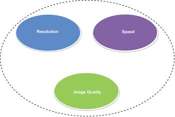
Three main attributes define the primary set of trade-offs for an area imaging device. The first set can be observed in imaging performance: image quality, maximum number of frames per second and resolution. The second set is in the functionality of the camera or sensor, where competing features call for difficult decisions. Examples of these secondary trade-off attributes include features such as windowing and power consumption. Finally, there are feasibility trade-offs dealing with cost, yield, reliability and other features related to the manufacturing of the imaging device.

CMOS image sensor primary trade-off. Images courtesy of Teledyne Dalsa.
Although in the past, image quality thresholds required the use of interline transfer CCD sensors in many applications, improvements in the design of CMOS sensors have led to better image quality and opened up new possibilities for much faster inspection systems with the desired image quality.
Historically, CCD interline transfer was the dominant sensor technology for shuttered imaging. The first generation of CMOS technology entered the market offering only rolling shutter functionality, which precluded its use in most shuttered applications, despite the opportunity for higher speed and lower power and cost. Later on, the CMOS global shutter feature was introduced, solving the rolling shutter shortfall and allowing CMOS to be relevant to more users. Recent advances have vastly reduced the noise and improved the signal-to-noise ratio levels in CMOS.

Distortion, rolling shutter and global shutter.
Now, in high-speed machine vision applications, CMOS meets or exceeds CCD interline transfer technology in functionality, performance and cost.
The latest generations of CMOS imaging technology have diminished the trade-off between resolution and speed by using very high data throughput, made possible by very fast, high-bandwidth analog-to-digital converters. The speed of these devices has challenged the boundaries of available data transmission standards such as Camera Link and has been the primary driving force behind the new high-bandwidth Camera Link HS standard.
Advances in pixel structures, such as global shutter pixels, have already narrowed the gap between speed and image quality, which in the past was an issue in high-speed applications. This technology currently is a de facto standard for any high-end CMOS image sensor.
Use of features such as pinned photo-diode technology and optimized implantation techniques reduces the dark current and number of “hot pixels” as well as the noise and lag in an image. This has improved the pixel signal-to-noise ratio. A lower noise floor means that new imagers can be used with less illumination at faster frame rates and still achieve the same image signal-to-noise ratio as older, slower, noisier designs.
The benefits of the new CMOS imaging technology are not confined only to the imaging sensor. Advances in CMOS camera design techniques also have offered new possibilities in terms of imaging performance. For example, real-time embedded processing in the camera compensates for non-idealities in the sensor, such as pixel response nonuniformity correction. This embedded processing also simplifies the vision system by performing processing that traditionally was done in a frame grabber, such as in-camera real-time flat-field correction. Windowing capability and the ability to change camera aspect ratio are other examples of how camera design in conjunction with a CMOS image sensor can provide additional capabilities to an end user.
Competing factors
When it comes to CMOS pixel structure design, a few fundamental competing factors define the performance of the CMOS imaging sensor. Some of these trade-offs are fundamental and physical, and some are due to non-idealities in the silicon or in the implementation of the device. In the past, a primary focus of CMOS technology development was overcoming image artifacts. The user must pay close attention to the performance of a CMOS image sensor with regard to artifacts arising in extreme situations, or related to certain operation and lighting situations. This consideration heavily affects a designer’s decision when faced with design trade-offs. A sensor with an excellent combination of specifications may prove to be unusable if it exhibits image artifacts.
Some of the major trade-off parameters are:
1. Fill factor: An inverse relationship exists between the number of transistors in a given pixel and its fill factor – the percentage of light-sensitive area in a pixel. Fill factor directly affects the sensitivity of a sensor and the signal-to-noise ratio of the captured image. On the other hand, having more transistors in a pixel allows for additional features that enhance image quality, such as global shutter and correlated double sampling.
2. Light acceptance angle: To minimize the impact of an increased number of transistors per pixel, most CMOS image sensors use microlenses to compensate for some of the lost real estate in a pixel due to the greater number of transistors. However, microlenses reduce the “light acceptance angle” in a pixel. Using microlenses somewhat improves the trade-off between the number of transistors in a pixel and image quality.
3. Pixel charge capacity (Qsat) and maximum exposure level: Another major drawback of having more transistors in a pixel is reduced pixel charge capacity. A reduction in pixel size (increased resolution for the same-size sensor) means less space for charge storage, which in turn results in lower pixel charge capacity. Reduced pixel capacity affects the suitability of sensors for some applications. For example, in the many that require the camera to differentiate between shades of gray in a bright image, shot noise is the decisive factor, not the absolute noise floor. Since the signal-to-noise ratio in the shot noise limit scales with the square root of the captured photon signal, shot-noise-limited applications require high pixel storage capacity. Higher pixel storage capacities also help to minimize the size and impact of several types of imager non-idealities, such as blooming and parasitic image artifacts.
4. Minimum exposure time, and resolution and power: Minimum exposure time directly defines the maximum practical speed of the imaging device. A sensor that is not optimally designed can exhibit image artifacts at low exposure times while behaving normally at longer ones. In a CMOS sensor design, the minimum exposure time is determined by the signal propagation speed within the sensor. Voltage stabilization could be compromised by suboptimal signal routing schemes. This issue becomes more evident as the sensor resolution increases. On the other hand, an ability to clock a sensor fast enough to capture a really short exposure time will also lead to larger exposure control feed-through artifacts as well as higher power consumption.

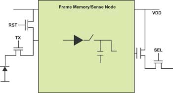
Voltage domain global shutter architecture.
5. Minimum achievable noise level: The minimum achievable noise level in a pixel is important in light-starved applications. Complex pixel circuitry and an increased number of stages can negatively affect the noise floor of a sensor. Essential techniques, such as correlated double sampling (a must-have feature to achieve equivalent or better noise figures as in CCD interline transfer devices), requires extra memory in the pixel architecture. This additional circuitry leaves less real estate in the pixel for light collection and signal storage, therefore limiting optical efficiency and maximum signal handling capacity.
There are a few schools of thought on how best to implement correlated double sampling in CMOS global shutter pixels. In general, “charge domain” techniques are superior to “voltage domain” techniques, but the former are more susceptible to shutter leakage.
6. Shutter leakage: When a CMOS pixel is read out, the charges from the light-sensitive area of the pixel are transferred to a storage area for subsequent charge to voltage conversion and data transfer. Because the storage area cannot be perfectly isolated from the imaging area of the pixel, unwanted signal may be collected in the storage node, creating parasitic image artifacts. To reduce this charge spillage, the charge can be immediately converted into voltage and sampled. This technique, also known as voltage domain global shutter, requires extra capacitors. However, the downsides of this technique are increased noise floor level relative to charge domain correlated double sampling and a negative impact on almost all of the previously mentioned performance parameters.
An alternative approach to the voltage domain global shutter structure is a charge domain structure, where the transfer of the image into a shielded area takes place in the charge domain. This vastly reduces the complexity of the pixel but requires optimized implementation of the components within a pixel. To achieve a better trade-off scheme between global shutter and other performance parameters, CMOS fabrication process challenges must be met and overcome. Essentially, with this method, a reduced number of high-quality elements in the pixel achieve the same result as a more complex pixel circuitry.
Meet the author
Behnam Rashidian is senior product manager at Teledyne Dalsa in Waterloo, Ontario, Canada; email: [email protected]. Eric Fox is technical director for CMOS ICs; email: [email protected].