PHILADELPHIA, March 15, 2006 -- Researchers at the University of Pennsylvania (Penn) announced that they have bridged a major obstruction in the creation of nanoscale electronics by developing a simple, reliable and observable method of creating microscopic gaps between electrodes.
 Such "nanogaps" will make it possible to make electrical contact to structures on the nanoscale, or billionths of a meter in size. Physicists Marija Drndic and Michael Fischbein created the nanogaps, which could have applications ranging from ultrafast electronics and quantum computing to high-speed gene reading.
"A number of people have proposed nanoelectronic devices that use nanogaps, but nobody has been able to create nanogaps reliably in practice," said Marija Drndic, an assistant professor in Penn's Department of Physics and Astronomy. "For the first time, we were able to make the world's smallest and cleanest nanometer gaps that can be imaged directly with atomic resolution. These nanogaps can be used to electrically connect small objects, such as an individual molecule."

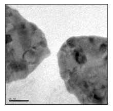
A TEM (transmission electron microscopy) image of a 5-nm nanogap taken from the research paper of University of Pennsylvania physicists Michael Fischbein and Marija Drndic, "Nanogaps by Direct Lithography for High-Resolution Imaging and Electronic Characterization of Nanostructures."
The ability to hook individual molecules -– whether they are the product of nanotechnology or biotechnology -– to electronic circuits is the goal of many researchers, the Penn physicists said. Such systems will have applications in medicine, robotics, materials science and even security. In addition, electronics on the nanoscale will be used to create denser, faster storage devices and microprocessor chips.
To create these gaps, Drndic and graduate student Michael Fischbein used electron beam lithography, a common nanotechnology tool that uses electrons to create patterns on a surface. Their research succeeded where previous efforts failed because of the type of surface they used -- thin layers of silicon nitride.
"Electon beam lithography works on a small scale, but it is limited down to about 10 nanometers." Drndic said. "It is not like drawing a line on a page; as an electron beam hits a material the electrons tend to scatter forward and backward, which makes it difficult to create tiny lines."
While other researchers focused on breaking small wires to create nanogaps, similar to how a fuse can be popped open, the Penn researchers said they went the opposite route, making the gaps directly.
"Contrary to many expectations, the thin layer of silicon nitride, which we used instead of the usual oxide on silicon, helped minimize the amount of electron scattering to the point where we could make clean gaps," Fischbein said.
Just as important, these nanogaps are compatible with high-resolution transmission electron microscopy, or HRTEM. Because nanogaps are created on thin films, it is easy to study the structure through HRTEM and assess their quality.
The researchers have used nanogaps to measure electrical charge through several coupled nanocrystals, which are also referred to as quantum dots. Previous researchers have demonstrated that quantum dots can be manipulated to change their physical properties, particularly their optical properties. In fact, the blue laser, which will soon be put into use in commercial products, was a result of early research in changing the colors of quantum dots.
"Nanogaps allow us to inject charge directly into individual nanocrystals, which may enable us to control their properties on a quantum level," Fischbein said. "It is a small gap, but across it we can bridge classical and quantum physics.”
The research was funded through grants from the National Science Foundation, the Office of Naval Research and the American Chemical Society. The project is described in a recent edition of the journal Applied Physics Letters.
For more information, visit: www.upenn.edu/researchatpenn