As CO2 lasers grow increasingly powerful, anti-reflective coatings are prone to failure. All-diamond optical windows featuring subwavelength surface structures show greater resilience and feature a higher laser-induced damage threshold.
ALEX MUHR AND GREG MULLIGAN, ELEMENT SIX
The explosion of demand in the telecom market in the 1990s spurred numerous advances in current and advanced coating methods. These developments led to denser coatings, featuring less porosity, and significantly cleaner coating chamber loading and unloading environments. With materials suppliers providing more pristine substrates, and coaters developing denser coatings, the industry developed faster and faster devices.
Other applications, such as cutting and drilling with CO2 lasers, also benefited from enhanced substrate and coatings. Initially when the CO2 laser’s efficiencies and high-power densities increased into the multikilowatt range, optical materials companies were forced to develop more internally pure products to manage power levels. As powers increased over the past 15 years, even higher quality substrates were required for handling the optical and thermal load.

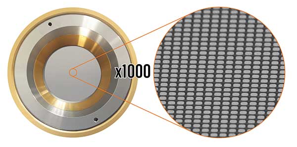
An up-close image of the Diamond PureOptics AR metasurface. Courtesy of Element Six.
With a combination of superlative thermal, mechanical and optical properties, diamond proved itself an ideal next-generation substrate. Furthering its adoption were the parallel advances made in the manufacture of large diamond windows using microwave-assisted chemical vapor deposition. Diamond’s wide transmission window from the UV through RF electromagnetic spectrum, combined with the highest hardness and thermal conductivity of any material, make it a standout material for robust optical applications. As a good example, it’s featured in extreme-ultraviolet (EUV) lithography, which uses a CO2 laser to generate sub−10 nm radiation.
AR coatings ‘weak link in the chain’
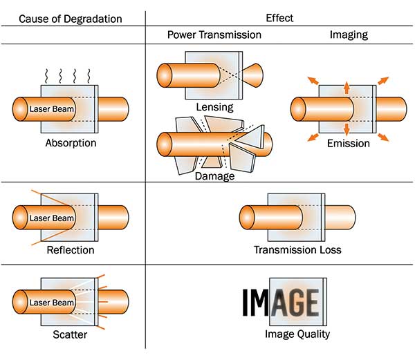
As light passes through an uncoated substrate, it is reflected at each interface; for reference, it’s approximately 4% for glass. This results in overall transmission of 92% or less for incident light. Applying anti-reflection (AR) coatings to each surface minimizes reflections and thereby increases transmission, reducing beam loss (Figure 1). AR coatings also reduce the potential for damage caused by reflections from optical surfaces traveling back into the original emanating system.

Figure 1. Mechanisms of beam degradation and their impact. Courtesy of Element Six.
To create reduced-reflection coatings, optical-matching from the substrate surface to ambient air is accomplished by depositing alternating high- and low-refractive index layers of dielectric materials in quarter- and half-wave thicknesses of the applicable wavelength. In CO2 laser systems, standard thin-film AR coatings take the diamond optics’ transmission from 71 percent to greater than 98 percent at the laser peak wavelength of 10.6 µm.
However, with many CO2 systems surpassing the 3 kW power level today, AR coatings on optical surfaces are no longer up to the task. These coatings, due to their material composition, have mechanical and thermal properties that are 1000× inferior to those of diamond itself.
This leads directly to increased thermal and mechanical failures as optical power densities increase. Even the process of handling and mounting an optic with a thin-film AR coating can compromise the coating’s mechanical integrity. This is the current ‘weak link in a chain’ of the optical beam train in high power laser optics.
In CO2 laser system applications, the most common failure mode for optical coatings results from the presence of absorption sites (small pits or foreign matter) within the coating layers or at the coating’s interface with the substrate or air. These absorption sites are usually in the form of gross defects that absorb laser energy, resulting in heat generation that causes localized melting or thermal stress factors. Failure by this effect is usually catastrophic. The common laser-induced damage threshold, or LIDT, that laser users are familiar with, describes the limits above which this type of damage to an optic can be expected.
Additionally, even if a thin-film coating can withstand the high power distribution of a laser, absorption of a portion of the
energy will occur within the coating itself. This absorption of laser energy will lead to heating and subsequent thermal expansion of the coating, which will in turn adversely affect the transmitted wavefront. This effect of absorption driven material expansion and wavefront distortion is known as thermal lensing. Repeated expansion and contraction of the thin-film coating can lead to delamination and ultimately catastrophic failure.
When irreversible damage occurs, costs to replace damaged optics can be very high.
As the system cannot run without the window, downtime (and associated costs and lost business), delivery and mounting of a replacement optic can be significant.
3D pyramids, 2D gratings reduce reflection
For these reasons, it is crucial for optical designers and engineers to be aware of absorption and potential failure sites within the coated elements of their system, and the alternative optical solutions that can eliminate these concerns.
Newer approaches for reducing reflections have been achieved by altering substrate surfaces with 3D pyramids or 2D grooves (gratings). These structured surfaces are often referred to as metasurfaces. When the incident wavelength is sufficiently larger than the features of these metasurfaces, the metasurfaces behave as a homogenous or continuous index film and reduce reflectivity.
Anti-reflective properties of metasurfaces have been evaluated for a wide range of size-to-wavelength ratios (including long- and short-wave limits) to find the optimal metasurface size. Until now, techniques for making these structures have been very difficult and costly, especially for higher power applications.
Researchers from Element Six and Harvard University took their cue from nature. They observed that nocturnal moths navigate under dim light thanks to eyes made of arrays of micro-sized lenses patterned with dome-shaped nanostructures. This allows the moth to see well in the dark, without reflection that could give away its location to predators.
The engineers developed an optic that mimics the structure of the moth’s eye, creating AR windows that consist purely of diamond, with no additional coating materials. The Diamond PureOptics AR metasurface works because the structured surface is smaller than the wavelength of light, suppressing any diffractive effects. Instead of diffracting, the light “sees” the surface as having a homogenous refractive index between that of diamond and the incident medium—in most cases air. When geometric parameters of the metasurface are optimized, the metasurface reduces reflectivity by acting much like a standard AR coating. The difference here is that the AR effects are produced from the same material as the substrate. There is no need to introduce inferior, nondiamond materials. As a result, the entire optic’s performance becomes dependent only on diamond’s outstanding intrinsic properties, which include the best thermal, mechanical and optical properties.
Semiconductor processing techniques
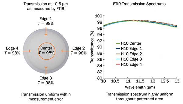
The manufacturing process has been developed through a collaborative effort between Element Six and Harvard University, capitalizing on the work of professor Marko Loncar at Harvard’s Center for Nanoscale Systems (CNS). This work builds on more than seven years of diamond-processing developments for applications ranging from photonic devices, sensing and, most applicably, high-power optics. A primary goal of this work has been the coupling of processing techniques and patterning variables to meet transmittance levels achieved by thin-film AR solutions today. To achieve this, conventional semiconductor processing techniques were used to create large area metasurfaces (>Ø40 mm) optimized specifically for the CO2 laser wavelength of 10.6 µm. These metasurfaces were applied to both sides of the diamond windows. Measurements by FTIR spectroscopy and CO2 laser have confirmed total window transmittance of >98% and reflectivity of <0.5% per surface (Figure 2).

Figure 2. Transmission of Diamond PureOptics AR. Courtesy of Element Six.
These results are in line with current anti-reflection coated optics at this wavelength. AR metasurfaces, despite being highly textured, do not lead to any increase in scattered light. Analysis of bi-directional scatter distribution function for uncoated diamond versus diamond metasurface AR windows showed no change in measured scatter.
Further, AR metasurfaces have been shown not to increase absorption either. This is in contrast to standard AR coatings at 10.6 µm, which typically absorb 0.1%
or more per coated surface. This absorption in AR coating layers, which possess relatively poor thermal and mechanical
properties, often leads to the development of hot spots, thermal lensing and potentially catastrophic failure. Replacing AR coatings with AR metasurfaces reduces overall absorption leading to lower operating temperature, less thermal lensing and greatly reduced potential for failure.
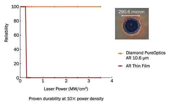
This leads back to the original discussion of providing the best optics for use in high-power laser systems. Specifically, experimental results have shown that replacing thin-film AR coatings with an all-diamond AR metasurface solution greatly increases the laser-induced damage threshold (LIDT), allowing much higher power densities to be transmitted through a window while maintaining low reflection losses. In a LIDT comparison test using a continuous wave laser at 10.6 µm, the LIDT of the thin-film coated window was determined to be 0.3 MW/cm2, while the same CW laser was unable to damage the Diamond PureOptics window even at power densities as high as 3.5 MW/cm2. This represents at least a tenfold improvement and possibly much more — enabling greater reliability and access to greater powers for lower cost customer performance.

Figure 3. Increased LIDT provides a more reliable solution. Courtesy of Element Six.
Long-time users of CO2 laser systems will recognize the resultant effects of failed optics in high power laser applications. By designing in these new AR metasurface windows, users can benefit from increased LIDT, higher reliability, longer component lifetime and reduced system downtime afforded by going with an all-diamond optical window (Figure 3). While synthetic CVD diamond optical substrates are already commonly used in high performance optical systems, AR thin-film dielectric coatings have become a limiting factor and need to be replaced with a better-performing solution.
Future efforts will focus on additional all-diamond solutions, including quarter-wave plates, filters and polarizers.
Meet the authors
Alex Muhr is an optical applications engineer at Element Six and has a master’s degree in applied physics from the University of Oregon; email: [email protected]. Greg Mulligan is the optics business development manager at Element Six. He holds a bachelor’s degree in physics from the University of California, Santa Barbara, and an MBA from University of California, Berkeley; email: [email protected].