The U.S. Naval Research Laboratory (NRL) executed a trade secret license to a silicon-nitride-based photonic component library to the Research Foundation for the State University of New York (RF SUNY), the administrator of AIM Photonics. By working closely with AIM Photonics’ foundry, the NRL’s Optical Sciences Division is developing photonic components with functionalities targeting Department of Defense (DOD) priorities such as analog signal processing, quantum information and computing, data remoting, and navigation and timing.
AIM Photonics is a DOD Manufacturing Innovation Institute.
“Photonic integrated circuits have demonstrated that combining optical sources, modulators, and detectors on semiconductor chips is a winning technology,” said Todd Stievater, a research physicist from the Photonics Technology Branch at the NRL and principal investigator. “They are already integral pieces of today’s internet data centers and enable the continued scale-up of the world’s flow of digital information.”
This success is founded in part on process design kits (PDKs), which include sets of pre-designed and pre-verified functional components for both traditional (electronic) integrated circuits and PICs.
“The RF SUNY license to NRL’s component library will permit AIM Photonics to create a new PDK for internal research and development by AIM Photonics customers,” said Nathan Tyndall, a research chemist from the NRL Photonics Technology Branch and co-inventor of the component library.

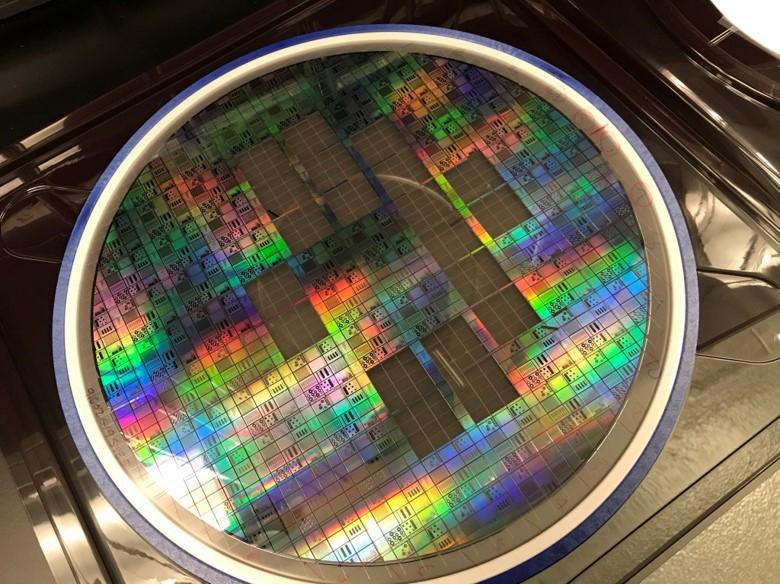
A 300-mm semiconductor wafer fabricated by AIM Photonics using a low-optical-loss passive fabrication technique and components developed by the NRL. The PIC semiconductor wafer is patterned into 64 identical parts, each one called a reticle, approximately 1 in. by 1 in. Twenty reticles have been removed from the wafer for analysis. Courtesy of the NRL Optical Sciences Division.
The Photonic Integrated Circuit Sensors program, which resulted in the creation of this intellectual property, is sponsored by the DOD’s undersecretary of defense for research and engineering, as part of the Trusted and Assured Microelectronics: Radio Frequency Opto Electronics portfolio. The component library is based on years of internal research at NRL focused on developing and processing silicon-nitride waveguides to support PIC applications. In NRL’s work, optical waveguides are formed in this material, which allow light to be transported across a semiconductor chip.
The high up-front labor and resource costs of PIC technology have hindered comparable development for lower-volume applications of vital interest to the Department of Defense,” Stievater said.
According to an NRL press release, with the exception of software, the Department of the Navy has not historically used trade secret law to protect its inventions, instead opting to protect its inventions under patent law. “While patenting offers the broadest scope of protection, it is also expensive, prolonged, and requires the invention to be publicly disclosed,” said Stephen Deese, an NRL Office of Technology Transfer partnership manager. “This is the first time a trade secret has been commercially licensed by the Navy and provides an additional tool to protect and license intellectual property.”
Trade secret law is less costly, quick to implement, and requires that the invention be kept secret. “Private sector companies routinely choose between trade secret protection and patent protection based on what makes sense for them,” said Sean Walsh, an NRL intellectual property attorney.
“New process technologies require new PDKs for designers to be able to take advantage of the technology. By partnering with experts like Dr. Stievater, we are able to move quickly to create and release a PDK with their verified photonic devices,” AIM Photonics COO David Harame said.
NRL’s component technologies, developed under this effort, are now available to license for companies with interests in collaborative research purposes, commercial applications, and educational partnerships.