The evolving technology of plasmonic nanophotonics seeks to combine the capabilities of nanotechnology and photonics.
Vladimir M. Shalaev, Purdue University, and Sergey I. Bozhevolnyi, Aalborg Universitet
Plasmonics has fascinated people for centuries, although they didn’t always fully understand its unique effects. During the Middle Ages, for example, infusions of colloidal metal particles in glass produced wondrously brilliant colors for cathedral windows. The colors were due to the excitation of plasmon oscillation modes in the metal particles, creating absorption bands and producing unique colors in the transmitted light.
As discussed last month in the first part of this feature, plasmonic materials are structures that support surface plasmon oscillation modes. In a metal, the conduction electrons are essentially free to move, with little interaction from their respective nuclei because of Coulomb shielding effects. The electric field of an incoming lightwave induces polarization of the conduction electrons with respect to the much heavier ionic cores of the metal atoms. At the surface of the metal, a net charge is produced. The net charge difference on the surface then acts as a restoring force for the polarization. As a result, the electrons oscillate coherently. If the frequency of the incident electromagnetic field is resonant with the coherent electron motion, a strong absorption in the spectrum is observed (see below).
Noble metals such as copper, silver and gold historically have dominated the studies of plasmon effects because their resonances are the strongest and occur in the visible part of the electromagnetic spectrum. Many structures support plasmon oscillations, however. Small metal spheres, such as those used in stained-glass windows, are one example. Others include thin, continuous metal films; random metal/dielectric films; nanoshells; nanowires; and lithographically produced metal arrays.
Sensing with plasmons
Surface plasmons can be employed for developing efficient biosensors. Biosensing, the detection and analysis of biomolecules such as proteins, has become an area of great interest for research as well as for applications such as environmental testing, national security, and process engineering and control.
One of the current biosensing methods is based on surface plasmon resonance,1 and it employs propagating surface plasmons at a metal/dielectric interface. In brief, a typical setup consists of a metal layer sandwiched between a high dielectric medium — e.g., a glass prism —and a medium with relatively low dielectric permittivity — in comparison with glass — such as air or a flow cell with biomolecules (Figure 1). Light is incident from the higher dielectric medium onto the metal surface.
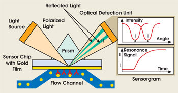
Figure 1. Surface plasmon resonance can be used to sense antibody-antigen binding by changes in the reflected intensity from the flow channel.
For a thin metal film, the evanescent field can penetrate from the metal/glass interface to the metal/low-dielectric interface, where it excites the surface plasmon. Note that, for any excitation frequency, the straight “light line” is above the ksp dispersion curve, and thus light cannot excite a surface plasmon at the metal/glass interface. This is because the longitudinal component of the lightwave vector in glass (SiO2), which is given by

(where θ is the angle of incidence), is always less than ksp at this interface. Hence, the required momentum conservation k|| = ksp cannot be fulfilled.
However, for the metal/low-dielectric interface (with εd < εSiO2), the surface plasmon has a smaller ksp, so the ksp dispersion curve for this interface can be above the light line in glass:

Thus, at a certain angle of incidence θ0, the momentum conservation condition can be fulfilled, and the surface plasmon is excited at the interface.
At the resonant angle θ0, a surface plasmon propagates along the surface within the flow cell. Hence, the intensity of the reflected light is smaller at the resonance because a portion of the incident energy is used for surface plasmon excitation.
When the resonance condition is destroyed, a measurable increase in the reflected intensity is generated (Figure 1, right). Even a very small change in the dielectric permittivity results in a detectable shift of the resonance condition. Therefore, the surface plasmon resonance technique enables the detection of minuscule changes in the flow channel. For example, it is sensitive enough to detect antibody-antigen (Ab-Ag) binding events, which are of great importance for performing bioassays, detecting disease biomarkers, and developing drugs and for use in many other biomedical applications.
Localized surface plasmon resonance also is highly sensitive to variations in the environment and thus can be used for the detection of antibody-antigen binding (Figure 2).2 The detection mechanism is similar to that in the surface plasmon resonance case above. The frequency of the localized surface plasmon resonance strongly depends on the environment. As an example, a localized surface plasmon resonance structure can experience a resonance shift of ~20 nm caused by Ab-Ag binding and, hence, can be employed as a very efficient biosensor. There is no dependence on the photon momentum because the structure is much smaller than the wavelength.
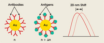
Figure 2. Localized surface plasmon resonance also may be used to detect antibody-antigen binding. The frequency is highly dependent on the environment, and a localized surface plasmon resonance structure can experience a resonance shift of approximately 20 nm in response to antibody-antigen binding.
Another important nanostructure that employs the localized surface plasmon resonance effect and can be used in many sensing applications is a nanoshell. Nanoshells are nanoparticles that consist of a dielectric core surrounded by a metal shell, typically gold. The resonance functionality mimics that of metal nanospheroids.
The localized surface plasmon resonance in nanoshells depends on the ratio of the dielectric core radius to the metal coating radius. It thus is an engineered parameter rather than the single resonance obtained from simple gold or silver nanoparticles. This can offer application benefits. For example, nanoshells designed to absorb at wavelengths near 820 nm could be used for in vivo techniques and controlled externally because tissue is relatively transparent at 820 nm.
Different from surface plasmon resonance or localized surface plasmon resonance, Raman scattering sensing techniques can not only detect the presence of a biomolecular analyte, but also provide a great deal of information on what material is being detected. Surface plasmons result in enhanced local fields, so they can dramatically enhance the Raman signal, which depends linearly on the local field intensity. Such surface-enhanced Raman scattering enables molecular “fingerprinting.”3
A detailed analysis of this powerful sensing technique is outside the scope of this article. We mention here only some recent and particularly efficient and sensitive surface-enhanced Raman scattering substrates. They include nanoshells developed by Naomi J. Halas’ group at Rice University in Houston,4 surface-enhanced Raman scattering substrates produced using nanosphere lithography by Richard P. Van Duyne’s team at Northwestern University in Evanston, Ill.,5 and adaptive silver films developed by Vladimir M. Shalaev’s group at Purdue University in West Lafayette, Ind.6

Figure 3. Field-emission scanning electron microscope images of two substrates from one batch illustrate a 12-nm silver film, with a transmission at 568 nm of 0.27 (a); a 12-nm silver film inside an antibody spot, with a transmission of 0.23 to 0.27 (b); and the same substrate as in (b) but inside an antigen (flag-BAP) spot, with a transmission of 0.4 (c). Images were collected eight weeks after fabrication; proteins were deposited one week after fabrication.
The adaptive silver films are fabricated at a certain range of deposition parameters, and they allow the fine rearrangement of their local structure under protein deposition (Figure 3). Such a substrate enhances surface-enhanced Raman scattering and makes possible protein sensing at a monolayer protein surface density. The silver substrates enable the “soft” adsorption of proteins without significant changes in their conformational states. The vacuum-evaporated films also allow label-free surface-enhanced Raman scattering detection of Ab-Ag binding.
Negative refraction
The photon is the ultimate messenger, packaging data in a signal of zero mass and unmatched speed. The refractive index is one of the most fundamental material characteristics influencing photons and their propagation. It provides the factor by which the phase velocity of light decreases in a material compared with vacuum conditions.
Of particular recent interest to researchers are materials that have a negative refractive index; that is, the phase velocity is directed against the flow of energy. There are no known naturally occurring examples of such materials. However, artificially designed structures — often referred to as “metamaterials” and involving plasmonic nanostructures — can act as if they have a negative index.
Metamaterials can open avenues to achieving unprecedented physical properties and functionalitiesthat are unattainable with natural materials. Because they bring the refractive index into a new domain of exploration, they promise to create entirely novel prospects for manipulating light, resulting in a revolutionary impact on optical technologies.
Materials can be characterized by a dielectric permittivity, ε = ε' + iε'', and a magnetic permeability, μ = μ' + iμ''. The real part (n') of the complex refractive index (n = n' + in''= εμ) will be negative in a passive medium provided that the condition ε'|μ| + μ'|ε| < 0 is fulfilled. The conditions ε' < 0 and μ' < 0 are sufficient (but not necessary) for negative refraction. Proof-of-principle experiments have shown that metamaterials can possess negative indices at microwave wavelengths.7
Negative-index materials drew a particularly large amount of attention after John B. Pendry of Imperial College London predicted that they could act as superlenses, enabling imaging resolutions that are limited not by wavelength but by material quality.8 This could result in a new family of devices for nano-photolithography and optical bioimaging. The near-field version of the superlens already has been reported.9
Although negative permittivity in the optical range is easy to attain for metals, there is no magnetic response for naturally occurring materials at such high frequencies. Recent experiments show that a magnetic response and negative permeability can be accomplished in the terahertz spectral ranges.10,11 Although negative refraction was not demonstrated, the work suggests the feasibility of developing materials with negative indices at optical frequencies because a magnetic response is a precursor for negative refraction.
The experimental realization of a negative refractive index for metamaterials in the optical range (at 1.5 μm) was accomplished with paired metal nanorods in a dielectric12 and then for the inverted system of paired dielectric voids in a metal.13 Inverted negative-index materials — i.e., elliptical or rectangular dielectric voids in metal films — are physically equivalent to paired metal rods in a dielectric host, in accordance with the Babinet principle. The first experimental observations of negative refractive indices at optical frequencies were based on earlier theoretical predictions.14 In parallel with the progress for metal/dielectric metamaterials, experimental demonstrations of negative refraction in the near-IR range have been made in photonic crystals.15,16
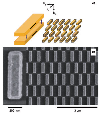
Figure 4. Optical negative-index material structures may be based on paired nanorods, as displayed in a schematic (a) and in an electron-beam fabricated sample (b).
The Shalaev group demonstrated an index of refraction of 20.3 at the telecommunications wavelength of 1.5 μm in pairs of gold nanorods, shown schematically in Figure 4a and as an electron-beam fabricated structure in Figure 4b. The twin nanowires form an open current loop with a resonant current, analogous to a telegraph line. Such a loop is “closed” through the displacement current and can support resonant modes for both the electrical and magnetic components of light, resulting in negative refractive indices for a range of visible and near-IR frequencies.
Recent progress in the fabrication and understanding of negative-index materials, followed by demonstrations of negative refraction first in the microwave and then in the optical ranges, provides the enabling science and technology for rapid advancements in this emerging area. There is an undeniable need for novel devices with the unique characteristics that can be provided by materials with negative indices. However, the understanding of the interaction of light with such materials is still in its infancy. Also, available optical negative-index materials are prone to losses. Thus, full integration of light with these unique materials requires fundamental advances in this research area.
In summary, the power of light is driving the photonics revolution, and the technologies formerly based on electronics increasingly enlist light to communicate and provide intelligent control. Plasmonic nanostructures can serve as optical couplers across the nano/micro interface, and recent advances in this rapidly developing area enable a systematic approach to the goal of full systems-level integration.
Acknowledgment
Vladimir M. Shalaev acknowledges help from Mark D. Thoreson in preparing this article.
Meet the authors
Vladimir M. Shalaev is the Robert and Anne Burnett professor of electrical and computer engineering at Purdue University in West Lafayette, Ind.; e-mail: [email protected].
Sergey I. Bozhevolnyi is a professor in the department of physics and nanotechnology at Aalborg Universitet in Denmark; e-mail: [email protected].
References
1. J. Homola, S.S. Yee and G. Gauglitz (Jan. 25, 1999). Surface plasmon resonance sensors: review. SENSOR. ACTUAT. B-CHEM., pp. 3-15.
2. G. Raschke et al (July 2003). Biomolecular recognition based on single gold nanoparticle light scattering. NANO LETT., pp. 935-938.
3. M. Moskovits (July 1985). Surface-enhanced spectroscopy. REV. MOD. PHYS., pp. 783-826.
4. E. Prodan et al (Oct. 17, 2003). A hybridization model for the plasmon response of complex nanostructures. SCIENCE, pp. 419-422.
5. C.L. Haynes and R.P. Van Duyne (July 2003). Dichroic optical properties of extended nanostructures fabricated using angle-resolved nanosphere lithography. NANO LETT., pp. 939-943.
6. V.P. Drachev et al (Aug. 30, 2005). Adaptive silver films for detection of antibody-antigen binding. LANGMUIR, pp. 8368-8373.
7. R.A. Shelby, D.R. Smith and S. Schultz (April 6, 2001). Experimental verification of a negative index of refraction. SCIENCE, pp. 77-79.
8. J.B. Pendry (Oct. 30, 2000). Negative refraction makes a perfect lens. PHYS. REV. LETT., pp. 3966-3969.
9. N. Fang et al (April 22, 2005). Sub-diffraction-limited optical imaging with a silver superlens. SCIENCE, pp. 534-537.
10. S. Linden et al (Nov. 19, 2004). Magnetic response of metamaterials at 100 terahertz. SCIENCE, pp. 1351-1353.
11. A.N. Grigorenko et al (Nov. 17, 2005). Nanofabricated media with negative permeability at visible frequencies. NATURE, pp. 335-338.
12. V.M. Shalaev et al (Dec. 15, 2005). Negative index of refraction in optical metamaterials. OPT. LETT., pp. 3356-3358.
13. S. Zhang et al (Sept. 23, 2005). Experimental demonstration of near-infrared negative-index materials. PHYS. REV. LETT., 137404.
14. V.A. Podolskiy, A.K. Sarychev and V.M. Shalaev (March 2002). Plasmon modes in metal nanowires and left-handed materials. J. NONLINEAR OPT. PHYS. MAT., pp. 65-74.
15. A. Berrier et al (Aug. 13, 2004). Negative refraction at infrared wavelengths in a two-dimensional photonic crystal. PHYS. REV. LETT., 073902.
16. E. Schonbrun et al (June 2005). Negative refraction in a Si-polymer photonic crystal membrane. IEEE PHOTONICS TECH. L., pp. 1196-1198.
Building Nanoantennae
Localized surface plasmons represent collective oscillations of free electrons in small metal nanoparticles, such as nanospheres or other nanoparticles and their groups. They concentrate energy in three dimensions within the nanoscale region.
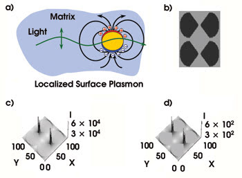
The localized surface plasmon on a metal sphere is shown (a). Bowtielike optical nanoantennae (b) display an enhanced local field in the gaps (c and d).
A localized surface plasmon acts as an optical nanoantenna with the metal, having negative permittivity εm, representing an optical inductive element and the dielectric host, which has positive εd, acting as optical capacitance.
By bringing two shaped metal nanostructures close together, one can create a particularly efficient bowtielike optical nanoantenna that can concentrate extremely large fields in the gaps between the particles.