The evolving field of nanophotonics seeks to combine the capabilities of nanotechnology and photonics.
Dr. Sergey I. Bozhevolnyi, Aalborg Universitet, and Vladimir M. Shalaev, Purdue University
In this first of two articles on optical technologies that manipulate photons at the nanoscale, we discuss how surface plasmons are analogous to photons and how they may be used to efficiently guide and control electromagnetic radiation. In at least some cases, surface plasmons enable dramatic improvements in the performance of conventional photonic components such as modulators and switches.
Nanotechnology may be loosely defined as a branch of engineering that deals with things that are smaller than 100 nm, especially involving the construction of structures from the bottom up by manipulating individual atoms and molecules. It is expected to strongly influence all technologies, from mechanical and electrical to the biological and medical, not only because these “things” are so small (imagine a nanosensor sitting inside the body measuring temperature, blood pressure, etc., and communicating with a remote hospital computer), but also because material properties and physical processes drastically change on these small scales. For example, carbon atoms can be arranged to make either coal or diamond, among other materials.
Photonics, although it deals with “ethereal” light, is not exempt from such effects on the nanoscale, and it can provide just as dramatic results.
Photonics is the science and technology of generating and controlling light particles (photons) and, in particular, of using light to carry information. It therefore deals with photons largely in the same manner that electronics deals with electrons. Photons are unmatched in speed (nothing beats the speed of light) and in their potential for data capacity (switching light on and off is easy because photons have no mass). The modern communications systems managing huge amounts of data and Internet traffic thus are based on glass fibers transmitting light signals worldwide.
Information processing at ever-increasing rates is evolving toward the use of nanophotonics. This involves not only very small photonic circuits and chips, but also new ways of sculpting the flow of light with nano-structures and nanoparticles that exhibit fascinating optical properties unseen in the macroscopic world.
Communicating at the nanoscale using light is a challenge. For most materials, interactions between light and matter are reduced when the size of the structures is much smaller than the wavelength of the light. There is a fundamental incompatibility between propagating light (e.g., in fibers) with microscale wavelengths and controlling light with nanoscale optical structures.
However, metals that support the surface collective oscillations of free electrons called surface plasmons can concentrate electromagnetic fields on the nanoscale while enhancing local field strengths by several orders of magnitude. For this reason, plasmonic nanostructures can serve both as nanophotonic components and as optical couplers across the nano/micro interface, acting as optical nanoantennae and dramatically enhancing the efficiency of light/matter interaction on the nanoscale (see “Understanding Surface Plasmons,” page 62).
Nanostructures using surface plasmons have been extensively investigated during the past decade. They exhibit a variety of novel effects, including extraordinary light transmission, giant field enhancement and surface plasmon waveguiding.1
Stripe guides
The conventional integrated optical devices used in optical communications for routing and switching light are based on the guiding of light in a dielectric waveguide, which consists of a high-refractive-index core and a low-index cladding. Electromagnetic radiation in the form of waveguide modes propagating in and confined to the core by virtue of total internal reflection can be controlled with externally applied electrical signals through electro-, magneto- and thermo-optic effects.
The controlling electrodes placed near the waveguides result in radiation loss by absorption and scattering. Increasing the separation between the electrodes and waveguide can minimize this loss, but that also decreases the useful effects. This makes the positioning of electrodes in conventional waveguide devices a challenging design problem.
Ideally, one would like to send the light and electrical signals along the same channel, facilitating information transfer from electronic to optical circuits. It turns out that thin metal stripes surrounded by a dielectric can be employed for both guiding radiation in the form of surface plasmon modes and for controlling its propagation; that is, modulation and switching.2,3
For a sufficiently thin metal film embedded in a dielectric, the surface plasmons associated with the upper and lower interfaces couple and form a symmetric mode (Figure 1a), propagating with loss as low as a few decibels per centimeter. Furthermore, a thin metal stripe surrounded by a dielectric (Figure 1b) supports the propagation of a surface plasmon stripe mode matching that of a single-mode fiber, facilitating efficient end-fire excitation (Figures 1c and 1d), typically with a loss of ≤0.5 dB.4
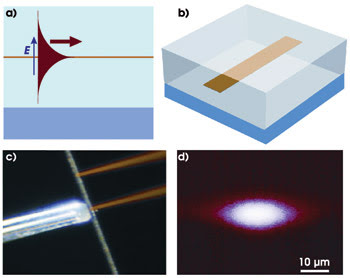
Figure 1. The surface plasmon mode field distribution near a thin metal film embedded in a dielectric is shown with the orientation of the dominant electric field component (a). A surface plasmon stripe waveguide was fabricated by sandwiching gold stripes between layers of polymer (b). An opticalmicroscope image of the end-fire in/out coupling arrangement shows a cleaved single-mode fiber and a fabricated sample with waveguide stripes (c). An optical microscope image reveals the intensity distribution of thefundamental surface plasmon mode at the output facet of a waveguide stripe excited at 1.55 μm (d).
Judging from the lateral mode distribution, such a surface plasmon stripe guide is similar to a conventional dielectric buried waveguide. It therefore is natural to recycle design ideas that are well-known in integrated optics and to apply them to surface-plasmon-based photonic components. Indeed, sharp and gradual (adiabatic) bends, Y-splitters, multimode interference junctions and directional couplers using surface plasmon stripe waveguides were demonstrated with overall performance similar to that of the best analogues from integrated optics.5
Unlike the cores of conventional waveguides, the metal stripes of surface plasmon guides also can carry electrical signals that affect the supported surface plasmon mode via material phenomena such as the thermo-optic effect. This has enabled the fabrication of devices such as a thermo-optic Mach-Zehnder interferometric modulator, a directional-coupler switch and an in-line extinction modulator, all of which use surface plasmon waveguiding along thin gold stripes embedded in a polymer and heated by electrical signal currents.
Interferometric modulator
The surface plasmon waveguides comprise gold stripes fabricated by UV lithography that are 15 nm thick and 8 μm wide, sandwiched between 15-μm-thick layers of benzocyclobutene (BCB) and supported by a silicon wafer. The fundamental surface plasmon mode in these stripes has a propagation loss of ~6 dB/cm and a coupling loss of ~0.5 dB at 1.51- to 1.62-μm telecommunications wavelengths when using end-fire in/out coupling with single-mode fibers. The radiation is guided along the metal stripe, with the field reaching its maximum value at the metal surface.
In general, polymers exhibit highly efficient thermo-optic effects.6 Heating the metal stripe that guides a surface plasmon is an efficient way to influence the polymer’s refractive index where the surface plasmon mode propagates and thereby control the mode propagation constant.
The generic operating principle of the Mach-Zehnder interferometric modulator is as follows: In the absence of a control signal, an input wave is split equally into two waves traveling along identical arms of the interferometer, which are recombined to produce an output wave. Ideally, the two waves meeting in the output junction are identical in phase and amplitude. When a control signal is applied to one of the modulator’s arms, the propagation of the corresponding wave is influenced via an optical material effect, causing its phase to lag so that the phases of the recombining waves are different at the output junction. If the waves are exactly out of phase, they cancel each other, and the result is zero output.
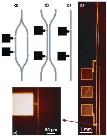
Figure 2. Schematics illustrate the structure of a Mach-Zehnder interferometric modulator (a), directional-coupler switch (b) and in-line extinction modulator (c).An optical microscope image of the fabricated Mach-Zehnder interferometric modulator shows stripes with typical bends (curvature radius >20 mm to ensure low bend loss), 100-nm-thick contact pads and connecting electrodes (d). A magnified image of the Mach-Zehnder modulator portion reveals an isolating 10-μm-long break (which does not introduce optical loss) in the waveguide stripe and a part of the thick electrode connected with a 20-μm-long, 15-nm-thick stripe to the waveguide (e).
In the thermo-optic Mach-Zehnder interferometric modulator (Figure 2a), the surface plasmon propagation constant is changed in the heated arm, resulting in a phase difference between two surface plasmon modes that interfere in the output Y-junction. A fabricated modulator demonstrating the approach was 20 mm long, with an arm separation of 250 μm. The active waveguide length was 5.7 mm. The total (fiber-to-fiber) insertion loss was measured at ~13 dB, the same as that of the reference stripe, and the structure exhibited excellent dynamic characteristics: 8 mW of electrical power was sufficient to obtain an extinction ratio of >35 dB with an exponential response time of ~0.7 ms (Figure 3).
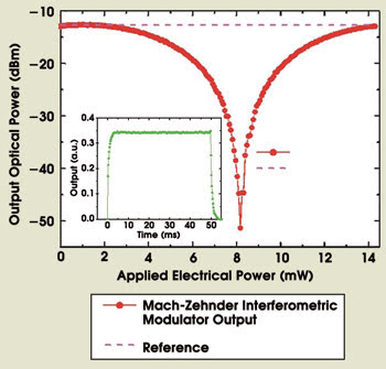
Figure 3. The driving power of the Mach-Zehnder interferometric modulator is considerably lower than that of a conventional, photonic device. The inset shows the temporal response of the modulator, measured with an offset of 2 V and a peak-to-peak voltage of 3.8 V. The electrode resistance was ~1.6 kΩ. Fitting exponential dependencies to the rise and fall of the modulator’s output power gives a response time constant of ~0.7 ms.
The achieved driving power is considerably lower than that of conventional photonic thermo-optic Mach-Zehnder interferometric modulators because the control electrode is positioned exactly at the maximum of the long-range surface plasmon mode field, inducing the maximum change in its effective index.6 Evaluating the dissipated heat, one obtains the following estimate for the driving power Pπ: (∂n/∂T)–1kwλ / d ≈ 7 mW, where ∂n/∂T (approximately –2.5 × 10⁻⁵/°C) is the thermo-optical coefficient of BCB, k (~0.2 W/mK) is the polymer’s thermal conductivity, w (8 μm) is the stripe width, w (15 μm) is the cladding thickness, and l (1.55 μm) is the wavelength.
This estimate is close to the measured value and indicates that using polymers with larger thermo-optic coefficients can decrease the driving power even further.
In a generic directional-coupler switch, two waveguides are in proximity over a portion of their length. As an input wave travels in one of the waveguides, it gradually tunnels into the other, which is identical in the absence of a control signal to the input side. The efficiency of this tunneling deteriorates if the two waveguides become different in the sense that the corresponding modes travel with different speeds. By controlling the propagation constant in one of the waveguides, one can completely stop the tunneling process. Hence, a directional-coupler switch can be used to efficiently switch radiation between the two waveguides at the output.
Proper operation of a directional-coupler switch (Figure 2b) requires that the radiation injected into one arm at the input efficiently tunnel into another arm in the interaction region where the arms are close enough for complete power transfer. Heating one of the arms induces a phase mismatch between the surface plasmon modes propagating in the coupled waveguides and thereby destroys efficient tunneling.
In a demonstration device with a stripe separation of 4 μm, the power transfer is efficient (~20 dB) at an interaction length of 0.9 mm. The corresponding directional-coupler switch was 15 mm long, and the best performance was obtained when the waveguide carrying the coupled radiation was heated: ~66 mW was needed to switch the optical power back to the excited waveguide, achieving an extinction ratio of >20 dB (Figure 4).
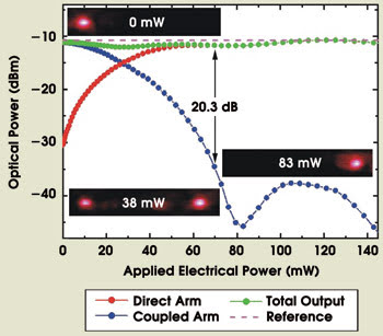
Figure 4. Without applied electrical current, the optical radiation is efficiently tunneled from the direct arm excited at the directional-coupler switch’s inputto the coupled arm. The insets show microscope images of the intensity distributions at the output facet of the switch (waveguide separation is 127 μm) for different values of applied electrical power.
The total insertion loss of the device was measured at slightly larger (~0.5 dB) than that of the reference stripe (~11 dB), and the temporal response was similar to that of the Mach-Zehnder interferometric modulator. The extinction ratio continued to increase for larger powers, reaching ~34 dB at 82 mW, and it stayed above 25 dB even at the first side lobe at 110 mW.
Optical switch
This switching behavior implies that the directional-coupler switch can be used as a digital optical switch, an attractive component for space-division switching in broadband photonic networks. Note that the driving power of the directional-coupler switch was larger than that of the Mach-Zehnder interferometric modulator because the switch’s electrode was 6 mm long and extended significantly over the tunneling region so as to decrease the total insertion loss when the electrode was heated. The electrode length can be optimized, considerably reducing the switching power.
In-line modulator
The refractive index of BCB (and other polymers) decreases when the polymer is heated (∂n/∂T <0). This suggests a simple configuration for intensity modulation (Fig. 2c), in which heating the waveguide stripe reduces the refractive index of the surrounding polymer and thus weakens the waveguiding effect of the metal stripe. Effectively, the heating destroys waveguiding and increases the radiation extinction in transmission, yielding an in-line extinction modulator.
The effective index of the surface plasmon mode supported by a 15-nm-thick gold film embedded in BCB (refractive index n ≈1.535 at 1.55 μm) can be evaluated to be Neff ≈ 1.5366. Assuming that the temperature increase needed to destroy waveguiding can be evaluated as ΔT = (∂n/∂T)–1(Neff – n) and using the same expression for the dissipated power as above, one obtains the power estimate P/L for the in-line extinction modulator: ~2k(∂n/∂T)–1(Neff – n)w/d ≈ 14 mW/mm.
Fabricated in-line extinction modulators were 10 mm long with an active waveguide and electrode length of 1 mm. The total insertion loss of ~8 dB was the same as that of the reference stripe, and an output power extinction of 10 dB was achieved with an applied electrical power of ~23 mW (Figure 5). This value can be regarded as reasonably close to the estimate because the latter does not refer to the extinction level, which depends on the surface plasmon mode divergence in the heated region.
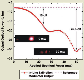
Figure 5. The in-line extinction modulator achieved an output power extinction ratio of 10 dB for applied electrical power of approximately 23 mW. An extinction ratio of more than 25 dB for 50 mW is feasible. The insets showmicroscope images of the intensity distributions at the output facet of themodulator for different values of applied electrical power.
A similar extinction ratio is expected even for a considerably shorter in-line extinction modulator (still having a 1-mm-long electrode), which suggests a method of reducing the propagation and, thereby, the total insertion loss. A 1.5-mm-long in-line extinction modulator with total (fiber-to-fiber) insertion loss of <2 dB and an extinction ratio of >25 dB for an applied power of 50 mW seems feasible, making this concept attractive for the design of compact variable optical attenuators that could be used to control power levels in telecommunications networks.
Finally, it should be emphasized that in-line extinction modulator operation depends weakly on wavelength, implying that the same modulator can be used in a broad range of wavelengths with proper adjustments to the applied electrical power.
The dynamic components discussed here represent the first use of the unique features inherent in surface plasmons that enable the same metal stripe to guide and efficiently control optical radiation. Taking into account that surface plasmon propagation loss can be reduced to on the order of 1 dB/cm and that the thermo-optic effect can be increased by several times through materials and processing optimization, the promising dynamic characteristics reported here can be significantly improved, making the demonstrated components attractive for use in telecommunications.
Moreover, the fact that surface plasmons are partially absorbed as they propagate along a metal stripe can be turned around and exploited to monitor the surface plasmon power.7 This can be accomplished simply by monitoring the stripe resistance, which is proportional to the temperature determined by the absorbed radiation, which in turn is proportional to the transmitted surface plasmon power.
Versatile design
Preliminary investigations indicate that the monitor sensitivity can be better than 10 μW, with the upper limit reaching 50 mW, covering a practical range of light powers used in telecommunications. Furthermore, the same design principles can be applied to configurations such as Y- and X-junction-based digital optical switches and variable optical attenuators.
The principles also can be modified to employ other control effects, including electro-optic ones. And it should be noted that surface plasmon components are based on true planar-processing technology, which considerably simplifies the development, large-scale integration and fabrication of photonic devices.
However, these components, although novel in design, are similar to their photonic analogues and relatively straightforward in operation. Many surface-plasmon-based structures, in contrast, are unique with regard to the principles of their operation and performance.
Next month, we will discuss this sort of plasmonic structure for nanophotonics, including biomolecular sensors and negative-index materials.
Meet the authors
Sergey I. Bozhevolnyi is a professor in the department of physics and nanotechnology at Aalborg Universitet in Denmark; e-mail: [email protected].
Vladimir M. Shalaev is the Robert and Anne Burnett professor of electrical and computer engineering at Purdue University in West Lafayette, Ind.; e-mail: [email protected].
References
1. W.L. Barnes, A. Dereux and T.W. Ebbesen (Aug. 14, 2003). Surface plasmon subwavelength optics. NATURE, pp. 824-830.
2. T. Nikolajsen, K. Leosson and S.I. Bozhevolnyi (Dec. 13, 2004). Surface plasmon polariton based modulators and switches operating at telecom wavelengths. APPL PHYS LETT, pp. 5833-5835.
3. T. Nikolajsen, K. Leosson and S.I. Bozhevolnyi (Jan. 3, 2005). In-line extinction modulator based on long-range surface plasmon polaritons. OPT COMMUN, pp. 455-459.
4. T. Nikolajsen et al (Feb. 3, 2003). (Polymer-based surface-plasmon-polariton stripe waveguides at telecommunications wavelengths. APPL PHYS LETT, pp. 668-670.
5. A. Boltasseva et al (January 2005). Integrated optical components utilizing long-range surface plasmon polaritons. J LIGHTWAVE TECHNOL, pp. 413-422.
6. H. Ma, A.K.-Y. Jen and L.R. Dalton (October 2002). Polymer-based optical waveguides: materials, processing, and devices. ADV MATER, pp. 1339-1365.
7. S.I. Bozhevolnyi, T. Nikolajsen and K. Leosson (Nov. 1, 2005). Integrated power monitor for long-range surface plasmon polaritons. OPT COMMUN, pp. 51-56.
Understanding Surface Plasmons
Light is composed of optical waves with a spatial period (the wavelength) that is determined by the refractive index of the medium through which the light is traveling. Surface plasmons are electromagnetic excitations that are bound to a metal/dielectric interface, and they represent optical waves coupled to free electron oscillations in metal.
Surface plasmons propagate along this interface, feeling the effects of both media. For this reason, the surface plasmon wavelength λsp depends on the properties of both materials at the interface through the dispersion relation:

where εm and εd are the dielectric permittivities of the metal and dielectric, respectively, and are important material parameters characterizing their optical responses.
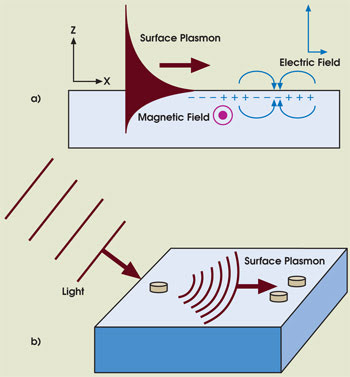
A schematic representation of a surface plasmon field distribution shows the orientation of the electric (blue) and magnetic (purple) fields (a). Various scenarios exist to couple long-wavelength light to short-wavelength surface plasmons that can interact efficiently with nanostructures (b).
The unique property of metals is that εm can be negative and wavelength-dependent. For dielectrics, εd is normally positive. At some frequency ωsp, the surface plasmon resonance condition εm (ω = ωsp) ~ – εd can be realized so that λsp becomes very short and can interact efficiently with and couple to nano-structures designed to realize various functionalities. In turn, a surface plasmon wave can be excited with a typical light source by using a nanostructure such as a nanoparticle placed at the metal surface.
Overall, surface plasmons represent unique electromagnetic waves that can have optical frequencies but very short (nanoscale) wavelengths, thus facilitating efficient coupling to nanostructures when one matches the small λsp to the size of the nanostructure.