Dr Martin Eibelhuber, Dr. Thomas Glinsner, Dr. Thomas Uhrmann and Paul Lindner, EV Group
The ability to create wafer-scale stitching-error-free patterns of nanostructures on bowed and warped surfaces and even on topography, as well as direct patterning of 3-D structures, makes nanoimprint lithography ideally suited for the needs of a diversified photonics market.
Photonics applications are emerging rapidly, thanks to the fabrication infrastructure of the semiconductor industry that enables new functionalities, smaller form factors, improved performance and reduced costs. However, the majority of today’s semiconductor technologies are used to develop electronics, which are based on controlling the flow of electrons, rather than on photons. Printing, or nanopatterning, of electronics is mainly a question of scaling to smaller geometries.
In contrast, developing the full potential of photonic devices depends on the nanoscale manipulation of light; shape and periodicity of the structures are the key parameters. For that reason, nanopatterning solutions will play an essential role in the photonics market.
Mature technologies such as photovoltaics, LEDs, laser diodes and optical sensors benefit from such light management, as it allows performance to be significantly enhanced by shaping the spectral response of absorption, transmission and reflectance. Furthermore, light-matter interaction can be tailored in many ways using structures like photonic crystals, gratings, phase-shift structures and waveguides, which allow photonic operations to be implemented on a single chip.
Silicon photonics has already demon-strated the potential of nanoscale photonic structures for improving Internet broadband/telecommunications by enabling increases in data transfer rates from rack to rack by orders of magnitude. Shaping the light-matter interaction in the nano-scale range is expected to have a comparable impact on the performance of other devices and applications, including medical health care and wearable devices that utilize micro-optoelectromechanical systems-based devices.
Photonics has a wide variety of applications, but many of these share common manufacturing needs. To this end, direct writing methods have been extensively used for research and development of optical structures. However, these techniques cannot be easily scaled up for cost-efficient production. Other writing methods, such as step-and-repeat optical lithography systems (steppers), are cost-effective when high-volume production is established but are designed for electronics, not the photonics industry. However, nanoimprint lithography (NIL), which in other industries has bridged the gap between R&D and high-volume manufacturing, can adapt to the needs of the fragmented and less standardized photonics market more easily. In particular, full-field UV-NIL can print patterns over large areas without stitching errors. The technique supports a wide range of structure sizes and shapes, including 3-D, and can even be used on high-topography (rough) surfaces, which can be an essential criterion for many photonic devices.
Steppers, which rely on pattern stitching because of limited field size, generally are used in LED manufacturing to produce patterned sapphire substrates (PSS). LEDs typically are produced by growing layers of gallium nitride (GaN) films on sapphire substrates, which are subsequently diced and packaged as individual devices. A key goal in LED manufacturing is to maximize light extraction, which is the amount of light emitted from the LED through the GaN layers. Much of that light is trapped within the GaN layer because of waveguiding effects. However, by patterning the surface of the substrate with structures, more light is scattered toward the top surface and directed outward from the device.1 In addition, these structures can improve the GaN growth process, resulting in thinner buffer layers and significantly lower dislocation densities.2
In addition to size and shape, another key parameter is the pitch between the patterns. If the patterning is done in a step-and-repeat process, as shown in Figure 1a, stitching errors at border areas commonly arise, even though actual pattern sizes are only within the micron range. Even minor variations in the order of the patterns result in significant pitch differences, which degrade device performance in these areas.
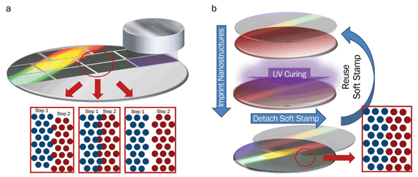
Figure 1. Comparison of step-and-repeat lithography with full-area NIL: (a) The step-and-repeat process results in critical areas between the patterned areas that give rise to different stitching errors shown in the inset. (b) The full-area nanoimprinting enables patterning that is free of stitching errors over the whole substrate.
Microscale PSS are already widely used in the production of high-brightness LEDs. However, using sapphire substrates with even smaller patterned structures, known as nanopatterned sapphire substrates (nPSS), can improve LED performance and reduce epitaxial costs even further.2 In particular, the emerging field of UV LEDs requires sapphire substrates with nPSS structures to address the smaller surface mobility associated with aluminum nitride (AlN) epi layers, which are needed to convert the emitting light to UV wavelengths.3 Although nPSS has already shown considerable advantages compared with PSS in terms of epitaxial growth and light extraction, widespread implementation is hindered by limitations with existing step-and-repeat patterning processes. Scaling down the size of the structures requires higher resolution and alignment accuracy performance from steppers – which results in increased production costs that are not sufficiently offset by the enhanced LED performance.
Steppers have limited illumination fields due to optical restrictions, but the resolution of NIL is not limited by field size. The master templates for NIL are written using very high resolution e-beam lithography at the required field size or even at the wafer scale. Subsequently, master templates are replicated by imprinting their pattern to a working stamp, which is used for the actual wafer processing. Using this method, the lifetime of the master template can be prolonged to be comparable to the lifetimes of masks used for optical lithography.
For the actual pattern transfer, a UV curable resist is applied to the substrate. The working stamp, which is transparent, then comes into contact with the substrate. Next, the resist is cured with UV light. Finally, the working stamp is released and reused for the next print. Such manufacturing methods, including the full-field UV-NIL technique described above and depicted in Figure 1b, allow efficient scaling down of structure sizes without introducing stitching errors or increasing costs significantly. Figure 2 shows that the ability to pattern nanostructures without stitching errors already has been proved on wafer diameters up to 6 in., which are currently used in LED manufacturing.
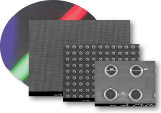
Figure 2. From millions to a few: Results of full-area nanoimprinted structures showing a 6-in. wafer down to scanning electron microscope images of single nanostructures.
The challenges that must be overcome for nPSS structures become even more important for purely photonic structures such as Bragg gratings and photonic crystals, where the optical response is defined by structure size and periodicity. Photonic crystals enable significant reductions in air-semiconductor interface losses, and they are considered particularly useful in enhancing the light extraction of high-brightness LEDs and the efficiency of photovoltaic cells.
UV-NIL patterning can be implemented with either hard or soft stamps. Hard stamps made of UV-transparent rigid materials allow higher alignment accuracy, but polymer-based soft stamps can more easily comply with nonuniform surfaces. When integrated with a soft-stamp capability, UV-NIL has the added advantage of being less sensitive to bowed and warped wafers compared to other patterning techniques, and can handle height differences much better than optical lithography. As noted above, steppers are strongly limited in depth of focus. This is particularly true when the critical dimensions of the features to be patterned are in the submicron range, which is required for photonics applications.
The high numerical aperture needed for critical dimensions in the submicron range causes the depth of focus of these systems to be on the order of only a few hundred nanometers. In contrast, UV-NIL enables the creation of structures down to sizes of less than 40 nm and, in conjunction with soft stamps (also referred to as “soft UV-NIL”), still accounts for height differences and creates patterns on topographical structures (Figure 3). Such nanostructures are desirable for implementing spectral filters in microspectrometers or gratings on light-guiding structures.
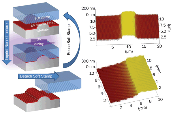
Figure 3. Process flow of nanopatterning on top of topographic structures using soft UV-NIL, with results measured by atomic force microscopy, showing highly uniform optical gratings on a prestructured substrate.
Standard optical lithography allows only the building up of structures layer by layer. This fits perfectly with the needs of the electronics industry but is not sufficient for manufacturing photonic structures. In contrast, soft UV-NIL enables the patterning of 3-D structures in a first-print process (Figure 4), which is ideally suited for the photonics industry,where light-matter interaction relies largely on shape and geometry. Since soft UV-NIL enables one to pattern different height levels in a single step, it eliminates the need for high alignment accuracy. The desired structures are imprinted into the resist and then transferred to the substrate by a subsequent etch step. As a result, the limitations of topographical patterning are only minor, such as the need to avoid structures with too large an undercut. Structures once fabricated by elaborate e-beam lithography can now be patterned using soft UV-NIL even in high-volume production, which facilitates the implementation of sophisticated photonic structures. This advantage adds a new degree of freedom for the design of photonic structures, as complexity does not necessarily result in high manufacturing costs.
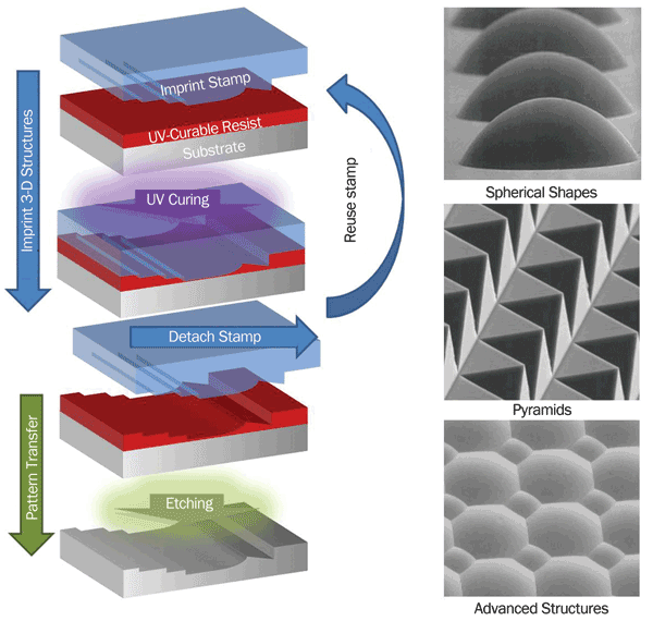
Figure 4. Process flow for pattern transfer of 3-D micro- and nanostructures with corresponding process results.
UV-NIL has also been demonstrated to enable 3-D structures that require a multiprint process, such as 3-D photonic crystals, as this kind of process can achieve high alignment accuracy – down to less than 100 nm – using standard optics.4,5 A 3-D photonic crystal is built up layer by layer, as depicted in the inset in Figure 5a. A large-area line-space grating is used, which is rotated 90° while creating the 3-D stack. In this case, alignment accuracies are critical to obtaining the desired device performance. Thus, in contrast to first-print processes where a soft stamp is preferred, a rigid stamp must be used.
Furthermore, to obtain improved alignment between the stacks, a two-stage alignment process is performed. First, proximity alignment is performed, followed by the moiré alignment. Overlaid moiré patterns are evaluated by gray-scale image processing (Figure 5b) to observe maxima and minima shifts, respectively, which are used to obtain excellent alignment of the layers to each other. In this case, optical alignment with accuracies down to several tens of nanometers is observed. As a result, a high-quality photonic crystal composed of five layers has been fabricated, as shown in the scanning electron microscope image in Figure 5a.
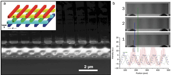
Figure 5. (a) Scanning electron microscope image of a 3-D photonic crystal with five layers fabricated by NIL with rigid stamps; (b) movement of the moiré patterns during the alignment procedure.
In an R&D environment, the fabrication of 3-D photonic crystals has been shown to be a simple and cost-efficient procedure.4,5 Although much work is still needed to commercialize 3-D photonic crystals, they can offer additional features such as optical nonlinearity, which is required to operate optical transistors. As a result, photonic crystals can play an important role in enabling future applications such as optical computing.
Meet the authors
Dr. Martin Eibelhuber is business development manager at EV Group in St. Florian, Austria; email: [email protected]. Dr. Thomas Glinsner is head of product management at EV Group; email: [email protected].
Dr. Thomas Uhrmann is business development manager at EV Group; email: [email protected]. Paul Lindner is executive technology director at EV Group; email: [email protected].
References
1. Y.C. Lee and S.H. Tu (2011). Improving the light-emitting efficiency of GaN LEDs using nanoimprint lithography. InTechOpen (doi: 10.5772/20712).
2. J.K. Huang et al (2013). Investigation and comparison of the GaN-based light-emitting diodes grown on high aspect ratio nano-cone and general micro-cone patterned sapphire substrate. J Disp Technol, Vol. 9, Issue 12 (doi: 10.1109/JDT.2013.2270276).
3. P. Dong et al (2013). 282-nm AlGaN-based deep ultraviolet light-emitting diodes with improved performance on nano-patterned sapphire substrates. Appl Phys Lett, Vol. 102, 241113 (doi: 10.1063/1.4812237).
4. T. Glinsner et al (2007). Fabrication of 3-D-photonic crystals via UV-nanoimprint lithography. J Vac Sci Technol B, Vol. 25, Issue 6 (doi: 10.1116/1.2798733).
5. M. Mühlberger et al (2007). A moiré method for high accuracy alignment in nanoimprint lithography. Microelectron Eng, Vol. 84, pp. 925-927 (doi: 10.1016/j.mee.2007.01.081).