Nanofilms Optimize Raman Thermometry for Extreme Manufacturing
Researchers at Iowa State University, Shenzhen University, and Shanghai University of Engineering Science demonstrated an approach to the thermal probing of nanomaterials in which the ratio of two resonance Raman peak intensities of a 2D material, tungsten disulfide (WS2), could be used as an indicator for high-sensitivity temperature measurements.
Traditional Raman spectroscopy-based temperature sensing typically tracks the change of Raman wave number, linewidth, and intensity. The temperature coefficients of these Raman properties are highly material-dependent and can be affected by local optical scattering.
The recently demonstrated thermal probing technique, called the Resonance Raman Ratio (R3) technique, precisely measured absolute temperature rise in nanomaterials.
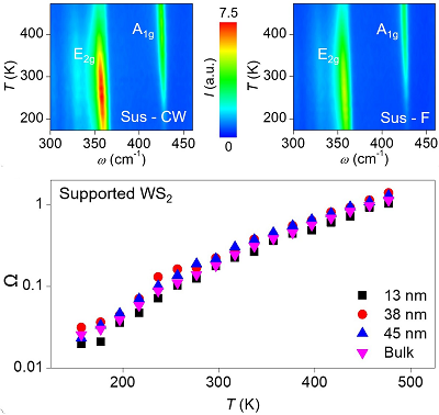
In experiments, the the intensity ratio of the two Raman peaks of WS2 — E2g and A1g — showed a universal behavior regardless of the material’s physical size, whether it was suspended or supported or whether it was nanometer-level or macrosize. The researchers used R3 to combine the temperature effects on resonance Raman scattering for the E2g and A1g modes.
The ratio showed a change in temperature from 177 K to 477 K.

When a nanometer-thick WS2 nanofilm undergoes resonance Raman scattering under 532-nm laser excitation, its two Raman peaks (E2g and A1g) have different variation behaviors against temperature, while the ratio (Ω = IA1g /IE2g ) shows universal behavior regardless of the sample structure (i.e., thickness; suspended or supported). This ratio changes by more than a hundredfold from 177 K to 477 K, demonstrating its robustness in high-sensitivity temperature probing. Courtesy of Hamidreza Zobeiri et al.
Using the ratio as the indicator, the researchers characterized the thermal diffusivity and thermal conductivity of suspended WS2 nanofilms via energy transport state-resolved Raman (ET-Raman). The results were in agreement with measurements made based on Raman wave number.
The researchers used a 532-nm laser (2.33 eV photon energy) to conduct the Raman experiment. The laser’s photon energy was close to the excitonic transition energy of WS2 at temperatures close to room temperature.
The R3 technique could broaden traditional approaches to Raman-based temperature measurement based on wave number shift, in addition to improving measurement sensitivity and robustness.
According to professor Xinwei Wang, the R3 method is superior to the classical wave number-based temperature measurement method for three reasons. First, since the intensity ratio is used, any optical focusing or optical interference-induced intensity shift is automatically eliminated in the ratio. This improves the robustness of the measurement.
Second, in many wave number-based methods, the Raman wave number becomes less sensitive to temperature changes at low temperatures, making the measurement less reliable. In contrast, the R3 method has an almost universal sensitivity from 177 K to 477 K. It would be possible to measure even lower temperatures with the R3 method by using materials whose bandgap change would increase intensity variation at lower temperatures.
Third, the R3 method makes WS2 a promising temperature sensor for measuring the temperatures of non-Raman active materials. The sensor’s temporal response is fast, making it attractive for temperature monitoring in extreme manufacturing.
“The R3 method truly opens a new avenue to study a material’s thermal response under either optical or other types of thermal loading,” professor Yangsu Xie said. “This will significantly improve our experimental capability of exploring nanoscale thermal transport physics, which is hard to probe using other techniques.” Xie is currently leading a study on thermal transport in nanoscale materials using Raman spectroscopy. “Also, the R3 method still holds the material-specific feature, so it makes it possible to achieve temperature probing of very well-defined physical domain.”
The method holds additional potential for use in microelectronics, according to Xie.
Although the work focused on R3 measurement using 532-nm laser-induced resonance Raman scattering, the researchers said it would be possible to use lasers of other wavelengths — for example, 633 nm, 488 nm, 785 nm — for resonance Raman scattering with materials having the same or closely matched bandgap.
The research was published in International Journal of Extreme Manufacturing (www.iopscience.iop.org/article/10.1088/2631-7990/ac6cb1).
Published: September 2022