GAITHERSBURG, Md., March 24, 2006 -- A state-of-the-art center for collaborative nanotechnology research will be set up at a facility of the National Institute of Standards and Technology (NIST), it was announced this week.
US Secretary of Commerce Carlos M. Gutierrez announced the project on Monday and said that scientists from US companies, universities and government will focus on overcoming major technical obstacles to cost-effective manufacturing of products made with components the size of atoms and molecules. He described the new center as an important and needed addition to the nation’s nanotechnology research efforts, according to an NIST press release.
“The national Center for Nanoscale Science and Technology (CNST) will help the private sector develop innovative products like more efficient batteries, lighter-weight and higher performing materials for aircraft and autos, and smaller computer chips to power digital devices,” he said. 
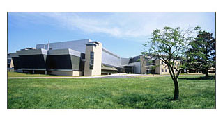
NIST’s Advanced Measurement Laboratory in Gaithersburg, Md., will house a new Center for Nanoscale Science and Technology and nanofab facility, it was announced this week. (Photo: Gail Porter/NIST)
The CNST features a growing research staff that will blend many types of specialized expertise, from physics and chemistry to mechanical engineering and computer science, he said.
CNST also houses a nanofabrication facility, or nanofab. This large cleanroom is equipped with a still-growing array of state-of-the-art tools for making, testing and characterizing prototype nanoscale devices and materials. These instruments will be available to collaborators and outside users.
Under the American Competitiveness Initiative, President George Bush has proposed a $20 million increase in funding for NIST’s nanotechnology research in fiscal year 2007. Part of the proposed increase would be used to speed the ramp-up of CNST research and services. 
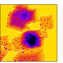
Better methods for high-resolution, three-dimensional chemical imaging of nanoscale structures, like these magnesium oxide cubes dotted with gold nanoparticles to help define surface contours, would be a boon to many areas of nanotechnology research and are an aim of CNST efforts. (Image: J. Bonevich/J.H. Scott, NIST)
CNST is based in NIST’s new Advanced Measurement Laboratory, which officials said is ideal for nanotechnology research because environmental influences, such as vibration or variation in temperature, can be controlled to extreme levels. CNST’s prime stated objective is to lay the technical groundwork necessary for US industry to make practical, manufacturable, market-ready products using nanotechnology. Through the CNST, partnering researchers also will have access to advanced measurement capabilities outside NIST's nanofab.
The CNST nanofab features state-of-the-art tools for electron beam- and photolithography, ion milling, electron and optical imaging, dry etching, metal deposition, wet chemistry, wafer preparation and optical and electrical measurements. The facility is expected to be available to outside users by late 2006. For more information, visit: http://cnst.nist.gov