Search
Menu
Lambda Research Optics, Inc. - DFO

NIL Technology Raises $31M to Scale Manufacturing

Facebook X LinkedIn Email
Flat optics developer NIL Technology (NILT) has raised €29 million (~$31.2 million) to help scale its manufacturing organization and capabilities. According to the company, with demand for its technology increasing, the company has matured its meta-optics technology from design to prototyping and is placing focus on bolstering its nano-imprint lithography (NIL)-based production process to meet higher-volume requests.
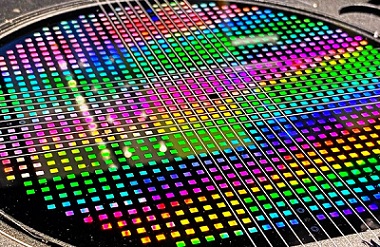
NILT’s manufacturing process fabricates wafers containing thousands of metasurface lenses (shown) using nanoimprint lithography. The company will use its recent funding to boost its manufacturing capabilities and capacity in order to meet rising demand. Courtesy of NIL Technology.
According to NILT, the NIL-based manufacturing strategy enables more precise and versatile nanostructures for higher performance meta-optics. High-volume production will be necessary to produce meta-optics for use in consumer electronics products such as smartphones and AR/VR headsets, and in automotive and robotics applications, the company said.

NIL Technology recently brought to market its MetaEye eye-tracking camera which targets applications in augmented reality, security, and sensing.

The funding was led by a group of investors including the Export & Investment Fund of Denmark, Jolt Capital, NGP Capital, and Swisscanto Private Equity.
Meadowlark Optics - Wave Plates 6/24 MR 2024


Published: May 2024
Glossary
wafer
In the context of electronics and semiconductor manufacturing, a wafer refers to a thin, flat disk or substrate made of a semiconducting material, usually crystalline silicon. Wafers serve as the foundation for the fabrication of integrated circuits (ICs), microelectromechanical systems (MEMS), and other microdevices. Here are key points regarding wafers: Material: Silicon is the most commonly used material for wafer fabrication due to its excellent semiconductor properties, high purity,...
lithography
Lithography is a key process used in microfabrication and semiconductor manufacturing to create intricate patterns on the surface of substrates, typically silicon wafers. It involves the transfer of a desired pattern onto a photosensitive material called a resist, which is coated onto the substrate. The resist is then selectively exposed to light or other radiation using a mask or reticle that contains the pattern of interest. The lithography process can be broadly categorized into several...
nanoimprint lithography
Nanoimprint lithography (NIL) is a nanolithography technique used for fabricating nanoscale patterns on a substrate. It is a high-resolution, high-throughput process that involves the mechanical deformation of a resist material on a substrate to create the desired nanostructures. The process is similar to traditional embossing, where a mold or template is pressed into a material to replicate a pattern. Here are the key elements and steps involved in nanoimprint lithography: Template/mold...
metalens
A metalens, short for "metasurface lens," is a type of optical lens that uses nanostructured materials to manipulate light at a subwavelength scale. Unlike traditional lenses made of glass or other transparent materials, metalenses do not rely on the curvature of their surface to refract or focus light. Instead, they use carefully engineered patterns of nanostructures, such as nanoscale antennas or dielectric structures, to control the phase and amplitude of light across the lens's surface....
meta-optics
Meta-optics, also known as metasurface optics or flat optics, is a branch of optics that involves the design, fabrication, and utilization of artificial structures called metasurfaces to control and manipulate light at the nanoscale level. Unlike traditional optics, which typically involve bulky lenses and mirrors, meta-optics aims to achieve similar functionalities using ultrathin, planar structures composed of subwavelength nanostructures. Metasurfaces are typically composed of arrays of...
BusinessOpticswafermanufacturinglithographynanoimprint lithographymetalensmeta-opticsfundingraisecapitalfundraisingNIL TechnologyNILTEuropeIndustry News

We use cookies to improve user experience and analyze our website traffic as stated in our Privacy Policy. By using this website, you agree to the use of cookies unless you have disabled them.