The integration of lidar into automotive applications is now pushing the boundaries of sensor, emitter and package design to exceed current specifications.
DENIS BOUDREAU, EXCELITAS TECHNOLOGIES CORP.
The defense industry, with its high performance and rugged environmental requirements, has long driven development of state-of-the-art technology platforms that have trickled down into commercial and consumer applications. The commercialization of military-grade technologies generally forces cost reductions, through process optimization and other means, to compete under open market conditions. However, the requirements in certain consumer applications are becoming more stringent and closer to those of military standard (mil-spec) uses. This is particularly true in the automotive sector, where the rise of driver assistance and autonomous vehicle technology — enabled by lidar platforms originally developed for military and defense — demands performance specs more closely matching the original military specs, insomuch as driver safety is at stake.

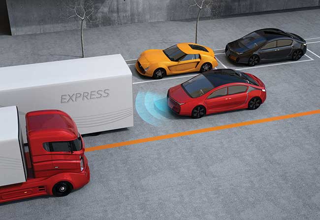
Lidar is already in use in civilian vehicles for automatic braking in collision-avoidance systems. Courtesy of cheskyw/123RF.
With rising demands on component and module performance, the design rules applied to lower-cost consumer-grade products need to be re-engineered. Considerations such as shock and vibration, performance in high humidity environments, and thermal management are all aspects of the design process that are affected.
Military standards have long defined how rugged components need to be in order to survive in harsh environments.
In the air, on the ground or at sea, conditions are very demanding — not only for the soldier but also for the supporting technology used.
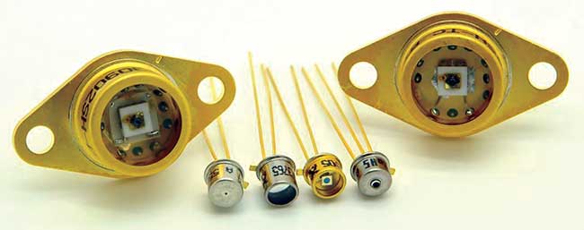
In the realm of optoelectronic components such as lasers and detectors, this has traditionally meant packaging the emitter or detector chip in a metal-can enclosure. Often referred to as TO (transistor outline) packages, these come in various industry standards such as TO-5 (8.1-mm cap diameter). The package consists of a header with pins onto which the chip is mounted, then wirebonded, then sealed under vacuum with a cap. This essentially seals the chip inside the package surrounded by an inert gas and protected from the environment. This type of package lends itself well to surviving various environmental conditions such as shock, vibration and temperature cycling, as well as high- and low-temperature operation.

Traditional fully hermetic TO (transistor outline) packages as used in military and other applications. Courtesy of Excelitas Technologies.
The construction of these packages comes with an inherently high cost that can limit their use in certain commercial applications. Even the defense industry is not immune to this reality, where commercial off-the-shelf devices are sourced when possible to avoid the higher cost of customization. In the consumer products world, including in automotive applications, cost constraints become mission critical.
Refinements in packaging
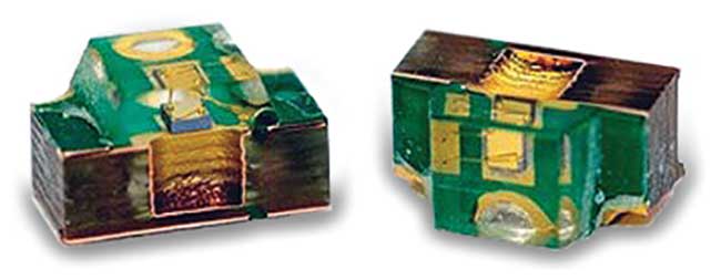
Packaging evolutions in the semiconductor world are now reaching the optoelectronics industry. In assembly plants today, most printed circuit board assemblies are assembled using pick-and-place robotic tools. Most components utilize surface-mount technology, which removes the need for solder wave processes and relies instead on reflow ovens to solder the various components.

New surface-mount device (SMD) packages allow significant component cost saving and volume manufacturing processes such as solder reflow without compromising reliability and performance. Courtesy of Excelitas Technologies.
For optoelectronic devices, one fundamental usage characteristic delayed the introduction of surface-mount packages: light. While an integrated circuit does not need to monitor its environment, the opto-electronic surface-mount package must support light transmission. This presents new challenges — when encapsulating avalanche photodiodes, for instance — as these detectors operate under high bias. Epoxies with high ionic content, for example, will see those charges get moved around by the high electric field and insert noise into the system. Careful selection and qualification of the chosen materials is critical in this case.
On the laser side, a different challenge arises where the very high light intensity exiting the device interacts with the encapsulation epoxy, which can cause localized heating and degradation of the facet. Once such challenges are surmounted, significant advantages in transitioning to surface-mount technology include the elimination of wave soldering needed for through-hole components, allowing a single reflow process for all components, reduced cost and more compact designs.
With the rise of autonomous vehicle technology, lidar has become one of the principal detection modes enabling the car’s vision. As in defense, the automotive industry sets very high standards for components to be qualified. In certain cases, the level of qualification that needs to be met is even higher.

New lidar systems will enable autonomous vehicles through the identification and tracking of other vehicles, pedestrians and unexpected objects in the space around the autonomous vehicle. Courtesy of iStock.com/chombosan.
This poses a particular challenge, as developers can no longer rely on the tried and tested TO package for reasons previously discussed. They now have to deal with application-specific environmental conditions that were well-managed by hermetic TO packages, primarily heat and humidity, using surface-mount packages instead.
Lidar components are separated into two product families — source emitter and detector. On the emitter side, very high intensity pulsed lasers are used, and on the detector side, avalanche photo-diodes (APDs) are commonly used due to their internal gain, which facilitates signal processing and improves signal-to-noise ratio (SNR). In automotive applications these systems are used in the forward-looking direction, with the laser pulses bouncing off of any target in front of the car. Typically that involves looking out in distances on the order of 200 meters. The light reflected off of the targets is then detected with high-sensitivity APDs, which gives the lidar system the basic data that it needs to reconstruct the image in software. When dealing with environmental conditions such as rain or fog, the drive electronics and software will influence performance, as will the chosen wavelength. Moving to 1550 nm from 905 nm, for example, will improve the transmission of the laser light due to varying water vapor absorption bands in the infrared. Background light levels are also lower at this wavelength, which further helps improve SNR. There are additional aspects to consider when selecting a system wavelength, as discussed further below.
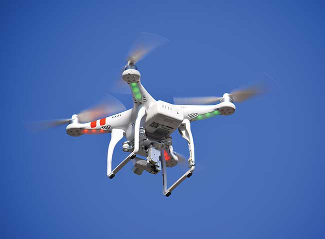
On the defense side, similar applications are growing in the unmanned aerial vehicles (UAVs) market space. Here, payload weight becomes an important consideration given the units’ need to maintain a certain level of maneuverability. The lidar system in these cases could be used for collision avoidance, landing assistance or terrain mapping.

A unmanned military drone using lidar for range-finding and terrain mapping. Courtesy of Daryl Knight/123RF.
Complete hermetic sealing is not possible in an epoxy-encapsulated surface-mount package, but careful selection of the epoxy material and proper design of the package will lead to highly reliable devices. At Excelitas, engineers run devices through very stringent life testing, including high-temperature and high-humidity testing for thousands of hours, before releasing a product to market.
Heat is also a challenge for epoxy-encapsulated devices; contrary to a TO can, there is no solid mass of metal that can dissipate heat from the environment or generated by the device itself. This is especially true in active devices such as pulsed lasers. A very short pulse, 10 ns for example, generates a lot of peak power (up to hundreds of Watts peak). Engineers must find a way to dissipate this heat away from the laser chip in order to keep its junction temperature at a minimum level to maximize reliability. Developing design rules of the substrate become critical in overcoming this challenge.
Another key factor of lidar systems is the wavelength of operation. The human eye can see from approximately 390 to 780 nm. This limits the use of these wavelengths in lidar systems for obvious reasons. Imagine every car in Los Angeles with red or green lasers guiding vehicles. Not only is this impractical, it is also an eye safety issue. The human eye is most prone to being damaged by these wavelengths, which it can see. Once outside of this range, there is still a risk, but you can illuminate the scene with higher power and still protect eye safety.
In legacy defense range-finding applications, and even today, 905 nm has been a wavelength of choice. Not only is it outside of the visible spectrum of the eye, it is very well matched to the peak responsivity of silicon detectors, making for an excellent pairing. For even greater usable power while retaining eye safety, systems are deployed at 1550 nm. This requires different materials for the detector, now moving away from silicon to InGaAs. From a system perspective, this has advantages, as it can be ranged further; however it does add cost. Processing InGaAs wafers is a more complicated, longer and more expensive process than silicon. This is another reason why current automotive lidar systems have converged around 905 nm. It’s believed, however, that future systems will eventually include longer wavelengths.
As capable as a human driver
Resolution comes into play in modern lidar systems. The ultimate goal of autonomous vehicles is to make the system as capable as a human being, without the risks caused by driver distraction. Beyond enhancing driver mobility, the ultimate goals are to reduce accidents and make the roads safer for all. Early lidar systems used point sources and detectors — in other words, one single emitter and one single detector. The engineers then had to mount multiples of these in a system, and somehow create a 3D image of the scene, such as rotating the assembly at fixed speed.
In more modern systems, OEMs are looking to use arrays of emitters and photodetectors for increased resolution. This provides multiple pixels of lasers or detectors all on the same structure, but also makes it even more challenging to get the heat out of the laser. The die mounting material needs a way to dissipate the heat, especially in systems where all pixels are fired at once. To reach the required price points, yields need to be high, as on a monolithic array; the overall yield of the die will be the single pixel yield to the power of the number of elements in the array. The substrate material selection also needs careful review to avoid warping for long and narrow arrays. All these design aspects must be considered in order to maintain both the performance and the long-term reliability of the component.
Optoelectronic packaging technologies have evolved over time, from legacy TO package devices in the defense industry
to small-form-factor surface-mount components for automotive uses. The common denominator is that both of these industries place very high emphasis on reliability standards. The integration of lidar into automotive applications is now pushing the boundaries of sensor, emitter and package design to ultimately meet or exceed similar specs at much lower price points for the consumer space.
Meet the author
Denis Boudreau is product leader of high-performance sensors at Excelitas Technologies Corp.; email: [email protected].