Daniel S. Burgess
A significant advance in atomic force microscopy (AFM) is at hand, thanks to a new type of probe that enables the acquisition of data on dynamic molecular interactions and the simultaneous collection of information about various material and surface properties. The probe is suitable for immediate use in existing AFM systems, and it may enable various novel imaging applications in fields from microelectronics to the biological sciences.

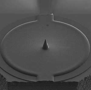
The new atomic force microscope probe incorporates an aluminum micromembrane. Tip displacement is detected by monitoring changes in the intensity of reflected diffraction orders from a grating deposited on the back face of the structure. Images courtesy of Georgia Institute of Technology.
The probe, developed by F. Levent Degertekin of the G.W. Woodruff School of Mechanical Engineering at Georgia Institute of Technology in Atlanta and colleagues at Georgia Tech and at Stanford University in California, integrates interferometric detection and electrostatic actuation in a microscale device. The result is a broadband, sensitive and fast force sensor.
Microphones to microscopes
Although Degertekin initially developed it for use in microphones and ultrasonic transducers, he said that he was inspired to apply the device to microscopy after Stanford’s Calvin F. Quate, one of the fathers of AFM, challenged the audience of his invited talk at a conference on scanning probe microscopy last June to solve a number of problems with the technique.
Degertekin approached Quate immediately after the talk with his potential solution, and the pair continued to discuss it over the next three days. Upon returning to Georgia Tech, the researchers built the probe and collected the proof-of-principle data they required in two hours.
“After I saw the first data come out in two hours, I couldn’t sleep for a week,” he said.
The probe features a 900-nm-thick, 150-μm-diameter aluminum membrane, to which a tip is attached. The membrane and tip are suspended above a quartz substrate onto which an aluminum diffraction grating has been deposited so that the cavity acts as a compact interferometer. The readout laser of a standard AFM illuminates the grating, and displacements of the tip caused by its interaction with the sample are detected in the changes in the intensity of the reflected diffraction orders. By using the grating as an actuator electrode, electrostatic forces can be applied to the membrane to adjust the distance of the tip from the sample as desired.


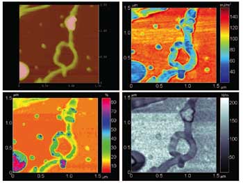
The probe enables the simultaneous collection of data on various material properties — such as topography, adhesion, contact time and stiffness — from one scan.
Degertekin noted that a unique characteristic of the probe is that it produces no background signal during tapping. Because it reveals the actual interaction forces on the tip, it essentially collects all sorts of information about the sample, he said, that can be analyzed to obtain details on its topography, adhesion, stiffness, capillary forces and viscoelasticity.
Moreover, electrostatic forces may be applied to the membrane to induce oscillations for fast tappingmode imaging and the generation of AFM movies. Previously, this imaging modality required complicated piezoelectric Z-axis translator, he said.
In demonstrations using the probe with a Dimension 3100 microscope equipped with a NanoScope controller, both from Veeco Instruments Inc. of Woodbury, N.Y., the scientists simultaneously collected peak attractive force and topography information from a checkerboard pattern of silicon, chromium and aluminum of varying thicknesses. They further produced fast-tapping-mode topography images of a calibration grating with 1-μm-wide, 20-nm-high steps and a 2-μm periodicity at line scan rates of up to 60 Hz, limited by the capabilities of the AFM.
Road to adoption
Degertekin plans to provide the probe to as many AFM users as possible so they may explore its potential. He suggested that promising applications include the evaluation of new dielectric films in microelectronic devices as they undergo thermal stress testing. Alternatively, he proposed that the tip could be replaced with a coating of functional molecules on the membrane to study dynamic biomolecular phenomena.
Although he said that he foresees no reason why microscopists would not adopt the probe, he conceded that its potential is currently limited by the capabilities of commercial AFMs. Specifically, the diffraction grating readout offers more sensitive signals in the various orders, but an AFM would have to be equipped with multiple photodetectors to collect that information simultaneously.
Review of Scientific Instruments, February 2006, 023501.