A Little Shake, Rattle and Roll
Hank Hogan, Contributing Editor
When it comes to the mechanical control of optical components, small, even microscopic, systems pack a big punch.
Researchers in academic and industrial laboratories are harnessing the power of microelectromechanical systems (MEMS) for use in tunable lasers, optical routers, variable optical attenuators, adaptive optics, displays and other devices.
Some of these devices are commercially available,
offered by a laundry list of companies, including Analog Devices Inc. of Norwood,
Mass.; Bandwidth9 Inc. of Fremont, Calif.; iolon Inc. of San Jose, Calif.; MegaSense
Inc. of Sunnyvale, Calif.; Nortel Networks Corp. of Brampton, Ontario, Canada; OMM
Inc. of San Diego; Onix Microsystems of Richmond, Calif.; and Texas Instruments
Inc. of Dallas. Almost all are built using silicon.
Except for those from Texas Instruments,
these companies’ devices are aimed at the telecommunications market. Putting
MEMS to work in this sector could significantly reduce the per-bit cost of transmission
and substantially boost the capabilities of photonic systems. However, it will require
solutions to several problems, such as the microscopic issue of stiction, which
can render parts impossible to move, and the difficulty of making the numerous and
necessary precision connections between the components in a system.
“If you are going to have the
MEMS mirror, you are going to probably want lenses, and you are going to want some
kind of a laser and some kind of a detector,” said Elsa Garmire, an engineering
professor at Dartmouth College in Hanover, N.H. “How do you put all of those
together in a system that is cheap to make, cheap and durable? I think that’s
a crucial problem to making optical MEMS successful.”
Finally, there is the macroscopic challenge
of funding. Because the proposed applications lie in telecom, the ongoing economic
train wreck in this sector may determine the future of optical MEMS. Industry observers
foresee a substantial risk of a large number of bankruptcies in the coming months.
That dims the short-term funding and market prospects for advanced devices.
Nevertheless, the longer-term prospects
still are considered excellent. In-Stat/MDR of Scottsdale,
Ariz., projects the market for MEMS in optical networking to grow from $33 million
in 2001 to $1.8 billion in 2006, said analyst Marlene Bourne. But there is the downturn
to weather, and the technology research firm does not expect things to turn around
until next year.
Tuning to the right wavelength
According to In-Stat/MDR, the primary applications
of micromechanics and optics will be in tunable lasers and variable optical attenuators.
The former is the domain of companies such as Nortel, iolon and Bandwidth9. The
latter is a specialty of MegaSense and its competitors.
Bandwidth9 lays claim to the largest
tunable laser manufacturing capacity in the industry in terms of raw wafers. Its
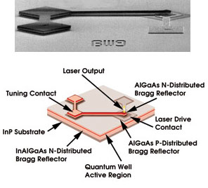
offerings include a device that incorporates a vertical-cavity surface-emitting
laser (VCSEL) and a MEMS cantilever (Figure 1). The 250-μm-long cantilever
hangs over the VCSEL to form one end of the resonant cavity. This cavity is much
shorter than the reach of the cantilever arm. An applied voltage moves the cantilever
by 0.5 to 0.7 μm, changing the length of the cavity and the laser’s output.
Once the desired wavelength is achieved, the output is sampled and controlled through
electronic feedback. This approach provides wavelength selectability through a 20-nm
band.

Figure 1. Bandwidth9’s
MEMS-based tunable VCSEL features a cantilever that forms one end of the resonant
cavity. An applied voltage moves the arm, changing the length of the cavity and
thereby tuning the output through a 20-nm band.
Companies such as Nortel and iolon
have similar capabilities. Nortel, for example, uses a movable mirror to change
cavity length, and iolon’s products employ a mirror on a rotator to change
the external cavity length. Bandwidth9 officials, however, claim that the company’s
monolithic growth process offers advantages over products that must be assembled.
Tunable lasers provide carriers with
flexibility. One tunable device can replace several fixed lasers, making it easier
to produce or repair the boards that drive photonic communications networks. Tunable
lasers also yield an immediate cost savings. “You’d have smaller inventory
because you wouldn’t have fixed lasers,” said John Fee, a vice president
at Washington’s WorldCom Inc. responsible for the beleaguered carrier’s
efforts in next-generation network architecture.
Other applications of tunable sources
involve the use of wavelength translation. To avoid network congestion, a signal
may arrive on one wavelength and need to go out on another because the first wavelength
is already in use. Variable optical attenuators and tunable bandpass filters, when
they become available, also could help boost network flexibility.
Fee said carriers believe that such
devices will be vital in the next-generation network. “It basically allows
you to tune your fixed optical network into a switched and wavelength-routed network,
which is the next step.”
These devices are not yet at the price/performance
point where they need to be, he said. Questions also remain concerning the scalability
and reliability of systems that are built on them.
Routing around bottlenecks
Another area where MEMS devices may be important
is in routing. Again, the sector is telecom, and the application is the optical
control of 1550-nm signals with very little loss.
These products are very different from
those used in other applications, such as Texas Instruments’ digital micromirror
devices for displays. For one thing, the mirrors tend to be quite large —
on the order of a millimeter.
The mirrors for telecom also tend to
be coated in gold because the metal is an excellent reflector in the infrared. Gold
can act like a dopant, however, and poison modern semiconductor circuits. One advantage
of MEMS is that the onboard electronics provide both the muscle to move things
and the brains to enhance device capabilities. Nevertheless, when gold is used,
great care must be taken in manufacturing to avoid inadvertently contaminating the
product and rendering the device dumb.
In a MEMS-based router, the optical
signal coming in on one fiber is sent out on another by altering the angle of the
mirrors between the input and the desired output path. Multiple wavelengths are
separated at the input, routed and then recombined at the output before continuing
their journey.
All-optical routing would get around
the bottleneck in switching. In current systems, the optical signals are converted
to electronic ones, directed to the appropriate path and converted back into infrared
radiation. This approach to switching inevitably constricts data rates.
But before all-optical routers are
viable, they must feature additional capabilities. Although a mirror-based system
can move the signals around, it cannot handle more complex tasks. For example, let’s
consider 10 signals running from New York to Los Angeles by way of Chicago. Dropping
a signal at Chicago and picking up another one can be done with mirrors, but it
is easier if optical elements are added.
“We’re moving away from
just plain, actuated micromirrors,” said Norman Tien, a professor at the University
of California, Davis, and co-director of the Berkeley Sensor and Actuator Center.
“They’re still going to be a component in the subsystem. For the tunable
add/drop multiplexer, you’re going to have to have a tunable filter.”
There are other problems to be overcome
with optical routing. Analog Devices’ MEMS mirrors are millimeters across,
partly because they have to interface with 8-μm-wide fiber cores. In the all-optical
system, a signal springs from a fiber core, travels a meter and must precisely re-enter
another fiber core. The task of aligning the core to the mirror and maintaining
that alignment is not easy, and switching requires changing that alignment quickly.
“It’s basically like taking
a rifle in Boston and hitting an egg in New York,” said Scott Blackstone of
Analog Devices. “It’s a pretty accurate thing. And they want to do
that in a few milliseconds — go from one position to another.”
Packaging, packaging, packaging
The company is among those that attack this problem
by putting intelligence in their MEMS components. Sophisticated electronics monitor
and control the movement of the mirrors to eliminate overshoot and oscillations.
This is especially important because an overdriven micromirror can become stuck
by stiction.
A larger issue is the number of inputs
and outputs. An optical switch may be routing hundreds or thousands of signals,
many arriving and departing as separate wavelengths in a fiber, resulting in complexity
— and expense. For example, there are packages with 1000 connections, arranged
like a choir in three rows. And every mirror, if it is to be individually managed,
requires a separate control signal.
 Optical inputs and outputs also must
be considered. Unlike electrical connections, they must be physically aligned, a
tedious process. And the small size of the MEMS-driven devices provides no relief.
“That is why packaging turns out to be such a nightmare and so expensive,”
said Olga Blum Spahn, a principal member of the technical staff at Sandia National
Laboratories in Albuquerque, N.M., and a leading optical MEMS researcher.
Micro-optoelectromechanics
The solution, and the ultimate future for MEMS-based
optical components, may emerge by following a road similar to the one taken by electronics.
Nearly 50 years ago, the transistor promised an electronic revolution, if the problem
of wiring the miniaturized components could be solved. The answer was found in the
integrated circuit, which combined many electronic elements into a monolithic and
easy-to-fabricate whole. The wiring was performed on-chip.
The analog in the optical world is
micro-optoelectromechanical systems, devices built out of the compound semiconductors
in optoelectronics. These systems are challenging to construct because of the nature
of the material and the limitations in processing. Compound semiconductors do not
yet have anything comparable to the surface micromachining responsible for the intricate
motors and gears found in some MEMS. So manufacturers can create devices designed
to move in only one dimension, such as a cantilevered arm.
However, whether built with compound
semiconductors or with some other material, micro-optoelectromechanical systems
promise to combine the optical, electrical and mechanical aspects of a system in
one package. The result would be an integrated photonic/electrical/mechanical assembly
that could solve many of the packaging problems.
As Sandia’s Spahn said, “If
you can do it monolithically, that would be wonderful, and so that is kind of our
goal.
The Optomechanical Effect
Although microelectromechanical devices are finding applications in the precise mechanical
control of optical components, light also can induce movement in various materials.
This optomechanical effect could power nanoactuators, micropumps and motors.
In the Sept. 19, 1997, issue of Science,
a team at Cambridge University in the UK described a semiconducting glass film
that reacted mechanically to polarized light. Made of arsenic and selenium, the
250-μm-thick film contracted or expanded depending on the polarization of light.
And in the July 2, 2001, Physical Review Letters, researchers from Albert
Ludwigs Universität Freiburg in Germany and Cambridge University reported
on their work with a rubbery material that shrank by as much as 75 percent when
exposed to ultraviolet radiation and that grew back in the dark.
In these two cases, the effect is thought
to be dependent on the microscopic structure of the material. In the case of the
glass, it is the arrangement of the atoms and the resulting interaction with the
electric vector of the polarized light. In the rubbery substance, it is the reshuffling
of molecular bonds.
Such optomechanical effects still are
under laboratory investigation, and commercial applications are likely years away.
However, if the effect does emerge from the lab, it may have some important uses.