The symbiotic relationship between metaoptics and optical metrology tools is leading to a rise in the use of metamaterials for commercial solutions as well as improved test and measurement techniques.
MARIE FREEBODY, CONTRIBUTING EDITOR
Meta- and nano-optics are on a fast track to a wide array of photonics systems and commercial solutions, enabling advancements that extend beyond the capabilities of more common and traditional optics. At the same time, owing to metaoptics’ dynamic physical and performance parameters, the convergence of optical metrology techniques with these optics is poised to reshape existing measurement protocols and pave the way for new approaches.
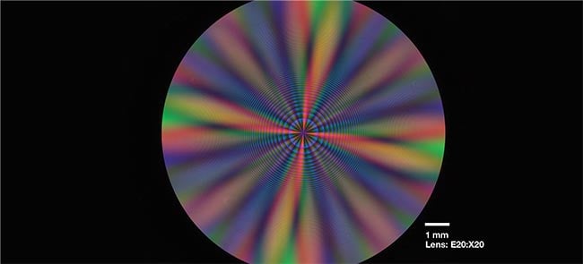
As metasurface characterization
opens the door to a heightened
understanding and new
application potential for these
optics, metaoptics, such as metalenses,
are also showing their
efficacy in adapting existing
measurement protocols. Courtesy of Moxtek.
Metasurfaces, the 2D subset of metamaterials, scatter and manipulate light in exceptional and sometimes unexpected ways. From their subwavelength thickness, engineers can use the structure of metaoptics to create components with previously unattainable properties. The field already attracts large-scale investments from companies such as Apple, Google, and Samsung. These tech giants are at various stages of marketing vision and imaging systems that provide consumers with previously unachievable features and performance in consumer electronics devices and solutions for authentication and telecommunications.
March to market
According to Valentin Genuer, field application manager at PHASICS Corp., a developer of wavefront sensors and optics testing stations, widespread excitement around metaoptics stems from the potential that the field holds to transform optical technologies by providing unparalleled control over light. The field, he said, enables the creation of optical devices that are both compact and versatile, with applications in various domains.
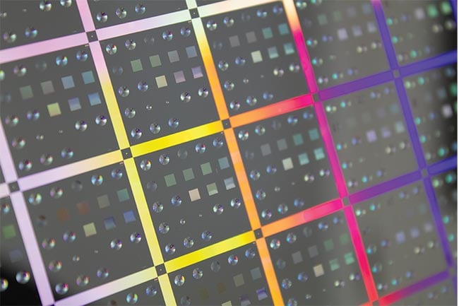
A 200-mm-diameter wafer with >1000 metalenses, each of which is designed and optimized for various optical systems. Courtesy of Moxtek.
It is also a field that benefits from the influence of stakeholders in multiple disciplines.
“The continual collaboration among researchers from physics, materials science, electrical engineering, and optics fosters ongoing innovation, leading to new breakthroughs and practical applications,”
Genuer said. As it relates to metamaterials for a company offering the capabilities of PHASICS, for example, opportunity exists in the need to qualify metaoptics and metasurfaces. This can be accomplished using wavefront sensing methodology to measure the nanostructures that compose metasurfaces.
Numerous research groups have reported advancements in metaoptics during the last decade. Upon demonstrating functional prototypes, the focus has shifted to working with optics fabs to produce volume levels for existing applications.
“The reason for the enormous commercial potential of metaoptics for high-
volume markets, such as consumer electronics, is that [they] can be manufactured with basically the same fabrication technology to make chips, based on deep-
ultraviolet lithography: CMOS-compatible metaoptics,” said Federico Capasso, the Robert L. Wallace Professor of
Applied Physics at Harvard University.
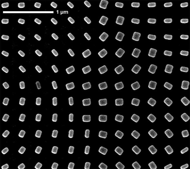
The micrograph section (top) shows a metasurface consisting of titanium dioxide nano-fins with a height of 600 nm. They are tiny waveguides (magnified, bottom) that exhibit structural birefringence due to their anisotropy. Visible light polarized along the short and long sides sees a different effective refractive index. A periodic array of this metasurface, combined with a lens and a CMOS sensor, forms an ultracompact single-shot polarization-sensitive camera capable of capturing, point by point, the polarization of a scene, including elliptical polarization. Courtesy of Harvard University/Federico Capasso and Noah Rubin.
“This is game-changing. Thus, the major chip foundries are now manufacturing metaoptics.”
A wave of commercial components using metasurfaces is on the market. Companies such as Metalenz (cofounded by Capasso), Moxtek, and NIL Technology are among the firms manufacturing metalenses. Applications span polarization imaging, microscopy, and biosensing.
Meanwhile, as this class of optics makes its mark on established applications, innovation continues in R&D settings. Capasso’s group, for example, has pioneered a class of polarization-sensitive cameras — which Capasso said are being used in two NASA projects. “This new camera principle, using a new metasurface polarization optic, has enabled Metalenz to demonstrate a new product, Polar ID, for secure face authentication,” Capasso said.
The use of the Capasso group’s polarization-sensitive metasurface in Metalenz’s PolarEyes camera allows for the creation of a smaller polarization camera, making the camera portable and a viable consumer device. Unlike traditional
polarization cameras that require a complex array of components to analyze Stokes parameters using amplitude or time division, a single metasurface does the job.
“In metaoptics you can have polarization-controlling elements — analyzers, polarizers, waveplates, etc. — that don’t use material birefringence, like standard polarization optics, but structural birefringence, also known as shape birefringence,” Capasso said. “Structural birefringence elements are, for example, rectangular nano-pillars, where light sees different effective [indices] when polarized along the two sides of the rectangle.”
Elsewhere in industry, semiconductor firm STMicroelectronics has partnered with Metalenz on a solution using metaoptics in facial recognition lidar
systems for cellphone cameras. Metaoptics imaging technology developer Tunoptix is developing visible and IR metalens designs, targeting a variety of camera sensor applications.
Still, the popularity and prowess of metaoptics does not necessarily indicate the nascence of this technology. For about 25 years, Utah-based nano- and micro-optics manufacturer Moxtek has mass-produced 1D periodic nanostructured metaoptic gratings, including wire-grid polarizers based on its Nanowire technology. The company uses a nanoimprint replication process to produce large-scale quantities of metasurfaces, which it aims to deploy for new applications due to integration-friendly form factors.
“This production capability allows Moxtek to capitalize on emerging metaoptic designs such as [metalenses] and other diffractive optical elements,” said Shaun Ogden, general manager at the company. According to Ogden, companies are evaluating Moxtek metaoptical components to replace or supplement existing conventional approaches.
Characterization: vital to market success
In the lifecycle of optical technologies,
metrology is essential not only as a final validation tool but also as an integral aspect of design and manufacturing processes. The early integration of metrology helps to ensure the manufacturability, scalability, and customization of these technologies, smoothing their transition from innovative concepts to mainstream applications. To move into the mainstream and support mass production in a cost-effective manner, highly precise and repeatable measurements must be able to be performed.
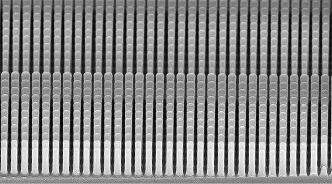
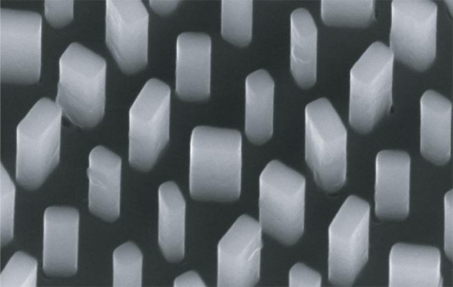
The shape and spacing of the meta-structures, shown as captured via a scanning electron microscope, are critical to achieve optimal performance. Among the metasurfaces that Utah-based Moxtek develops are metalenses, metaoptical elements, and diffractive optical elements. Courtesy of Moxtek.
Metrology of metaoptics poses significant challenges due to the specialized nanofabrication required for these materials. Traditional test and measurement methods are apt to fall short in accurately capturing the detailed functionalities of these advanced materials.
Metrology tool designers are addressing this bottleneck. “The availability of research-grade metaoptic metrology tools is supporting the growing commercial success of metaoptics,” Ogden said. “However, the limited test speed of the current tools needs improvement to support high-volume production. Rapid, specialized, wafer-scale metrology tools will be required as volumes continue to ramp.”
Metaoptics designed for visible and near-IR wavelengths require submicron feature sizes with precise tolerances and tightly controlled production processes. At volume production scales, a single wafer may contain hundreds or even thousands of small metaoptics. So, the sheer volume of measurements required for commercialization places major demands on test and measurement tools.
“The number one need is for quality
control to be applied in the most automated way, in situ, and in real time, so that faults and imperfections can be identified quickly and efficiently,” said Themos Kallos, cofounder and chief science officer of nanotechnology and functional materials company Meta Materials Inc. (META).
“The main challenge is that nanoscale resolution is required but over large surface areas (around 1 m in length). The depth of the metasurface features can be 10 nm, so this needs to be measured across a length that is 100-m-times larger than the depth.”
New measurement capabilities
Producers of lens measurement devices that are actively developing and enhancing tool sets to better measure metaoptics must balance the need to perform accurate measurements at both low and commercial volumes. Moxtek, for example, currently uses a TRIOPTICS ImageMaster measurement test station. It plans to switch to TRIOPTICS’ higher-volume tool.
According to Kallos, several key advancements are already underway that are serving to improve metrology for real-world applications — including those using metaoptics. “First is enhanced resolution, to distinguish the nano-features usually present in metaoptics structures; second is real-time, in situ monitoring, for example, adapting the methods for a production environment, not just the laboratory,” Kallos said.
“And third is scalability, which means being able to offer quality control over large surface areas and large volumes.”
While metrological concerns may hinder aspects of the commercialization of metaoptics, they have also kickstarted innovations that enhance the commercial viability of these technologies. For as much as metrology considerations are essential to the sustained adoption of metaoptical technologies, metaoptics themselves are valuable elements to characterizations elsewhere in the optics value chain.
One example is characterizing focusing efficiency. Conventional lens manufacturers may not perform measurements for focusing efficiency, because significant losses in these lenses owe mainly to surface reflections. For metalenses, in which considerations to physical structure vary considerably from conventional lenses, characterizing focusing efficiency is highly important. Metalens-specific metrology approaches must also be able to capture higher-order focal spot information and zero-order leakage.
To perform this operation, spectrally filtered light is used to illuminate an object using a pinhole or cross aperture. A conventional lens collimates the light from the object and sends the light toward a metalens. The metalens then focuses this light to recreate the object image at its focal plane. Next, a microscope objective is focused onto the same focal plane as the metalens, and the recreated object image is recorded and analyzed to determine the performance of the lens. By adjusting the position of the objective lens, data can also be collected for zero-order and higher-order modes.
“Another method is to illuminate the meta-element with collimated light and project the transmitted light on a scattering screen that can be recorded by a camera,” said Daniel Bacon-Brown, an engineer at Moxtek. “This can be useful for studying meta-elements that are nonfocusing, such as diffraction gratings and structured light generators.”
Metasurfaces also find application in interferometry. A light beam that is transmitted through a metasurface is combined with a second reference beam of the same wavelength. Differences in the pattern of diffraction can be linked to differences in the phase inflicted by the metasurface at a particular location.
According to Kallos, the challenge in this application is to scan a large surface area.
“The interferometric beam needs to be scanned using a movable mirror system, for example, or expanded to cover a large area, then the diffraction pattern imaged onto a sensor,” Kallos said.
Evaluating such vast quantities of data may require advanced image processing to distinguish signal variations created by interference caused by the metasurface phase change at a particular location. This change is due to signal variations that stem from the spatially varying structure of a metasurface.
PHASICS’ interferometric systems
are based on a nonpolarization-dependent and achromatic approach. “This interferometric method and the way we implement it in our instruments make it well adapted to the metrology of metaoptics,” Genuer said. “Our main instrument is a camera-like device suitable for in situ measurements. Instead of having to bring the samples/wafer to a metrology room, one can perform measurement in situ or at least very close to the manufacturing line.”
Application considerations
The efforts of product engineers as well as researchers and developers have advanced the application of metasurfaces to optical metrology problems in recent years. The importance of compact components and devices to the constant pursuit of improved levels of precision and control in the optical domain increases the likelihood that a new generation of optical metrology engineers, trained in nanophotonics, will transfer their knowledge and designs into industrial applications. For example, polarization-based optical
metrology could benefit from better polarization components that are thinner, exhibit higher polarization contrast, and/or have tighter retardance deviation.
Metasurfaces can already be viewed as a natural evolution of some of the optical components currently used in industrial metrology, such as diffraction gratings. Photolithography company ASML, for example, uses diffraction gratings to carry out overlay metrology between two layers on a chip with an accuracy down to 1 nm in metrology systems used in the semiconductor industry.
“Such metrology targets, currently based on gratings, can be engineered using metasurface concepts for added value [including] higher accuracy, other materials, and smaller feature sizes,” said Alberto Curto, a professor at Ghent University and imec. “We have seen impressive demonstrations of displacement sensors with angstrom resolution and related work with single particles, high-finesse meta-mirrors, and, more broadly, the development of picophotonics.”
Curto pegs the semiconductor industry as the perfect real-world setting to develop and deploy metasurfaces for optical metrology. “Metasurfaces can be naturally incorporated into wafers as metrology targets,” Curto said. “It is an industry that uses typical metasurface materials, such as silicon, with a high refractive index, plasmonic metals, like aluminum or silver, and dielectrics, like silica.”
Further, metasurfaces are used for optimized edge detection in analog image processing. Typically, in these cases, a light source illuminates a mask that creates an image that is then “processed” by the metasurface. The resulting image of the mask is used to confirm the sharp edges in real-time optical images, all without the need for a digital computer. According to Kallos at Meta Materials,
this science remains an early-stage laboratory concept and deployment, he said, is considered a possibility in the next decade.
Looking forward
Broadly, metamaterials experts who are pursuing applications in metrology stress that more awareness is needed in industry to consider the possibilities offered by both metasurfaces and nanophotonics for designing advanced optical metrology systems. The development of national metrology institutes and the efforts that these institutes would drive would also bolster efforts.
“In-depth engineering is needed to
tailor metasurfaces for a specific metrology application, because the potential
design space is so vast,” Curto said. “From the academic side, it is also necessary to listen to the metrology needs of companies that could potentially benefit from a metasurface-based solution.”
These types of dialogues are just now beginning, Curto said.
From within industry, while it is widely understood that the proliferation of advanced optical designs necessitates new measurement capabilities, realizing necessary protocols is a challenge.
Volume production again takes top priority.
“I’m not sure completely new methods can adapt fast enough to industrial scales, but existing ones can be more easily improved,” Kallos said. “New product types require adapting optical metrology techniques, such as spectroscopy, ellipsometry, interferometry, and laser scanning confocal microscopy to characterize the features of the metasurfaces at scale.”
Capasso agrees that, in general, the same techniques used in the metrology of refractive and diffractive optics can be used in and with metaoptics. He also believes that research on harnessing the distinct capabilities of the metasurface itself can enhance the accuracy of metrology beyond the performance of conventional optics.