Bob Wang, Mike Ward, Rick Rockwell and Jennifer List
As a practical matter, residual birefringence is supplanting intrinsic birefringence
as a more important parameter for product quality control.
In recent years,
leading-edge optical lithography has been moving to ever-shorter wavelengths: from
248 nm (KrF excimer laser) to 193 nm (ArF excimer laser) and now to 157 nm (F2 excimer
laser). At 157 nm, calcium fluoride (CaF2) is the primary lens material used in
step-and-scan systems because of its optical properties and its readiness for mass
production.
These systems require extremely high quality material.
Three parameters are especially critical: low absorption, high homogeneity of index
of refraction and low-level linear birefringence, which we will hereafter call simply
birefringence. This last parameter in particular has taken on increased significance
with the push toward shorter wavelengths.
Exploring birefringence
Birefringence is an anisotropy in refractive indices
along different crystal axes when working with linearly polarized light.1 For example,
calcite, one of the most common uniaxial crystals in polarization optics, has two
principal indices of refraction. CaF2 is a single crystal belonging to the cubic
group characterized by a high degree of symmetry (four- and threefold rotation axes).
One assumption used to be that single
crystals in the cubic group have isotropic optical properties, particularly, the
index of refraction.1 Last year, however, John Burnett and colleagues at the National
Institute of Standards and Technology in Gaithersburg, Md., determined the intrinsic
birefringence in CaF2 at 157 nm to be Δn = —110 — n001 = -1.12 x 10—6, or
11.2 ±0.4 nm/cm.
The scientists believe this intrinsic
birefringence at short wavelengths comes from a symmetry-breaking effect of the
finite wave vector of the photon on the symmetry of the light-matter interaction
in cubic crystals.2,3 This level of birefringence is more than 10 times higher than
the tolerance of the optical lithography industry. Only by applying complicated
correction designs is the industry able to reduce the effect of intrinsic birefringence
to an acceptable level.4
Stress factors
Besides intrinsic birefringence, external mechanical
stress or residual stress in bulk materials, which may be introduced during the
materials’ growth and production phase, can also induce birefringence via
the photoelastic effect. The increasingly stringent requirements for low-aberration
optics used in step-and-scan systems have mandated improved specifications and control
of birefringence at extremely low levels (preferably <0.5 nm/cm).
Although positioning optical components
at different crystal orientations can correct for intrinsic birefringence, this
is not the case for residual birefringence, which is subsequently emerging as a
more critical parameter for product quality control.
For industrial quality control, instead
of using Δn, it is easier to express birefringence according to retardation
magnitude (nm) and fast-axis angle. It also is possible to normalize retardation
to the thickness of the sample (nm/cm) through which the light beam passes. The
relationship between retardation values δ (nm), Δn and the thickness
of the measured sample, D (cm), is
δ (nm) = Δn x D (cm)x 107.
Since the discovery of intrinsic birefringence
at 157 nm, the optical lithography industry has developed a critical interest in
measuring birefringence at that and other lithography wavelengths. In response to
this need, International Sematech awarded Hinds Instruments a contract to expedite
the development of a deep-UV birefringence measurement system to characterize birefringence
in CaF2 at 157 nm.
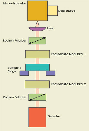
The resulting deep-UV birefringence
measurement system uses a deuterium lamp as the light source and a monochromator
to select the wavelength, with the light from that device collimated by a CaF2 lens
(Figure 1). The lens is followed by a Rochon polarizer at —45°, a photoelastic
modulator at 0°, a sample mounted on an X-Y scanning stage, another photoelastic
modulator at 45°, another Rochon polarizer at 90° and, finally, a photomultiplier
tube. The optical train arrangement is vertical to minimize any birefringence that
horizontal mounting might induce. All of the optical components reside in a nitrogen
environment (O2 < 10 ppm) because oxygen absorbs light at 157 nm.

Figure 1. The optical setup of the deep-UV
birefringence measurement system developed at Hinds is vertical to eliminate any
birefringence induced by horizontal mounting of the sample.
The electronic signals generated at
the detector have both AC and DC components. The AC signal containing the birefringence
information is processed using two lock-in amplifiers. The equipment processes the
DC signal, representing the average light intensity reaching the detector, using
a special function of one of the two lock-in amplifiers, which is equivalent to
passing the detector signal through an electronic low-pass filter and an analog-to-digital
converter. A PC records resulting data and calculates retardation magnitude and
fast-axis angle.
The key optical components in the instrument
are the photo-elastic modulators.5 Such resonant devices produce polarization modulation
of a light beam with a precise sinusoidal waveform. This, in turn, provides high
sensitivity and accuracy in measuring birefringence.6
The system can measure birefringence
in any optical material transparent at 248, 193 or 157 nm.7 This includes quantification
of both residual and intrinsic birefringence problems. In-house testing indicates
the device also provides high repeatability (3 σ/mean <1 percent) at a
low noise level (0.01 nm).
To determine the noise level of the
system, we first took a series of measurements with no sample present. This data
set of approximately 450 data points gives an average of 0.0092 nm and a standard
deviation of 0.0046 nm.7 To test the repeatability, we measured samples at different
retardation levels repeatedly at fixed sampling spots. The data set of more than
400 data points has a mean of 5.64 nm and a standard deviation of 0.014 nm. The
3 σ (three times the standard deviation) value is about 0.7 percent of the
mean for this test, which represents a high level of instrumental repeatability.
Furthermore, the measured fast-axis angles of the same sample are within ±0.1°.
Mapping birefringence
Using the deep-UV birefringence measurement system
called Exicor, researchers have mapped the retardation of several CaF2 cubes at
157 (Figure 2a), 193 and 248 nm (Figure 2b). In these maps, the light beams were
propagating along the (110) axis, this being the orientation in which the intrinsic
birefringence (n—110 — n001) is measured. The birefringence map at 193 nm has a
similar birefringence pattern.

Figure 2. Birefringence maps indicate magnitude and fast-axis angle of a CaF2 cube measured
at (a) 157, (b) 248 and (c) 633 nm, with light propagating along the (110) crystal
axis.
It is important to note that the 157-nm
map illustrates a sample with significant variation in retardation values. The 441
data points have an average retardation value of 27.0 nm (or 11.3 nm/cm), a maximum
value of 29.2 nm (or 12.2 nm/cm), a minimum value of 25.0 nm (or 10.5 nm/cm) and
a standard deviation of 0.8 nm. The retardation varies as much as ±8 percent
from the average value. If not handled properly, such a high level of retardation
variation will affect how accurately one can determine the intrinsic birefringence
in CaF2 at 157 nm.
In principle, the intrinsic birefringence
in a single crystal should be constant at a given wavelength. The observed variation
in retardation values over the scanned areas could result from the presence of both
intrinsic and residual birefringence in the CaF2 cubes measured.
If it is assumed that the residual
birefringence in a sample is random, then sufficient averaging over a large number
of data points should minimize the contribution of residual birefringence. The average
of 441 data points measured at 157, 193 and 248 nm leads to average values of normalized
retardation of 11.3, 3.55 and 1.13 nm/cm, respectively. These data are in good general
agreement with the previously reported values.
The birefringence map measured at
633 nm using a HeNe birefringence measurement system (Figure 2c) illustrates dramatically
different birefringence patterns from the other images, particularly with regard
to fast-axis angles. There is a somewhat random angular distribution, with localized
areas of high retardation dominated by angles around 0° (for example, the two
high-retardation ridges at the low right corner) and 90° (for example, near
the central area). In contrast, fast-axis angles around 0° (horizontal) dominate
the other images. The irregularity of the fast-axis angles for the 633-nm map also
indicates a dominance of residual birefringence. The average of 441 data points
measured at 633 nm leads to a low averaged value of normalized retardation of 0.258
nm/cm. The intrinsic birefringence in CaF2 should become much smaller at 633 nm,
according to the 1/—λ2 dependence.
The 633-nm map helps explain what is
happening in the other images. The two high-retardation ridges in its lower right
corner (presumably residual birefringence) appear as high-retardation ridges in
the other images, because the fast-axis angles in those two ridges are nearly parallel
to the fast-axis angles of the intrinsic birefringence. At 633 nm, the fast-axis
angles in the central area of the sample are closer to vertical than horizontal.
Therefore, it appears that residual birefringence with a fast-axis orientation close
to 90° cancels a substantial portion of the intrinsic birefringence, which
is shown as lower retardation regions in the other images.

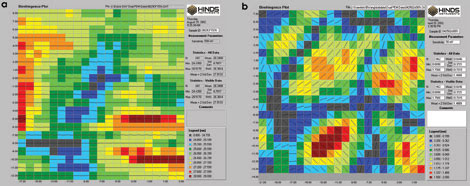
Figure 3. Figures 3a and b. Besides mapping with light propagating along the
(110) crystal axis, scientists also mapped residual birefringence at 157 nm in CaF2
samples at nonintrinsic birefringence crystal axes. The difference in birefringence
quality is obvious from even a cursory examination of the two data maps.
This instrumental approach also allowed
mapping of residual birefringence at 157 nm in a variety of CaF2 samples with the
light beam propagating along (111) and (100) crystal axes (Figures 3a and b, respectively).
Here we see two examples with average retardation values of 5.44 nm (1/4-in.
thickness) and 0.66 nm (1-in. thickness), respectively. The difference in birefringence
quality is obvious from even a cursory examination of the two data maps, and illustrates
the measurement system’s capability as an at-wavelength tool for quality control
of lens materials that are used in 157-nm optical lithography.
References
1. E. Hecht and A. Zajac (1974). OPTICS,
Addison-Wesley, London, p. 251.
2. J.H. Burnett, Z.H. Levine and E.L.
Shirley (2001). PHYS. REV. B, 64 241102(R).
3. J.H. Burnett, Z.H. Levine, E.L.
Shirley and J.H. Bruning, JM3, in print (2002).
4. N. Shiraishi, et al (2002). Progress
of Nikon’s F2 exposure tool development. Proc. SPIE, Vol. 4691, p.
594.
5. J.C. Kemp (1969). J. Opt. Sci.
Amer. 59, p. 950.
6. B. Wang and T.C. Oakberg (1999).
REV. SCI. INSTRUM. 70, p. 3847.
7. B. Wang (September 2002). Exicor
DUV birefringence measurement system at optical lithography wavelengths. Third
International Symposium on 157-nm Lithography.
Acknowledgments
This project has partial funding from International
Sematech. The authors would like to thank John Burnett at the National Institute
of Standards and Technology for his valuable discussions and for offering samples,
and the entire Hinds team involved in developing the birefringence measurement system
for their help.
Meet the authors
Bob Wang, Rick Rockwell and Jennifer List are
with the Applications Research Group of Hinds Instruments Inc. in Hillsboro, Ore.
Mike Ward is the marketing manager.