Confocal microscopy can handle the measurements involved in complex ultraprecise manufacturing and inspection.
Michael Metzger, Nikon Instruments Inc.
Since the early 1900s, science and industry professionals have been using optical measurement and inspection for a clearer view of their products for research, development and manufacturing. These techniques of observing, measuring and analyzing product components are undergoing dramatic changes as semiconductor technology is implemented in innovative and imaginative ways.
Today we need a measurement system at the next level of precision to keep up with higher performance demands in the semiconductor packaging market and to address the trend driving the development of ever-smaller components.
Higher circuit density means increasing complexity in packages. Measurement of multilayer chips and of the position and height of the wire and microbump connecting the layers is critical. Furthermore, the fusion of these technologies requires high accuracy, high speed and precise measurement for three-dimensional structures of differing materials.
Solving the measuring problems inherent in 3-D coordinate semiconductor packaging requires:
• Resolution enabling consistent height measurement.
• Processing cycle times adequate for high-throughput measurements of the entire package.
• Accuracy of better than 1 μm.
• Simultaneous measurement of reflection ratios from 1 to 100 percent.
Confocal accuracy
Widely used in bioscience research, confocal microscopy offers several advantages over conventional optical microscopy, including controllable depth of field, elimination of image degradation from out-of-focus information and the ability to collect serial Z-axis optical sections. The confocal approach uses spatial filtering to eliminate out-of-focus flare in samples thicker than the focus plane.
Confocal microscopy’s various imaging modes rely on techniques needed to produce high-resolution images (optical sections) in sequence. For instance, biology might require data from sections in single-, double-, triple- or multiple-wavelength illumination modes.
Nikon Instruments recently developed a confocal measuring head for industrial applications that require fast and accurate height measurement, such as the complex materials found in medical and semiconductor devices.
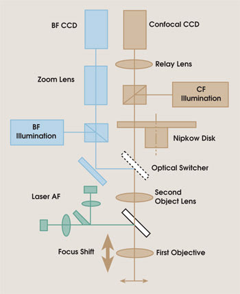
The measuring head uses a Nipkow disk, a type of scanning disk with many symmetrically placed spirals of pinhole apertures through which illumination passes to be split. When the disk spins, the light scans the sample in a raster pattern, with each beam emerging from a pinhole to scan across a portion of the field. Light from the sample then projects onto a digital CCD camera.

The confocal measuring head for industrial applications incorporates a Nipkow disk. A second optical path offers the capabilities of a conventional vision system, such as edge detection, coordinate measurement and laser scanning. BF CCD = bright-field CCD.
Previously, the most common way to achieve micron-level Z-axis measurements in industrial imaging was to use high optical magnification (greater than 500×). This is because micron-level Z-axis accuracy requires lenses with at least a 0.3-μm depth of field, and the shallow depth of field requires higher magnification lenses. However, the ultrahigh magnification reduces the field of view, which drops for the X- and Y-axes to as small as 160 μm for a 500× optical system (50× objective lens).
Therefore, when examining a large semiconductor device, the Nipkow confocal microscope’s wider field of view — as much as 8000 μm for the X- and Y-axes — decreases imaging time by covering more real estate in each shot.
Another problem in micron-scale industrial imaging is that obtaining accurate height measurements requires control of reflected light. Different reflection rates complicate measurement for different materials.
In confocal imaging, however, moving the objective lens along the optical path also shifts the confocal optical plane. The position of the focal plane and of the sample surface is the point at which the strongest reflected light captures the image. The image itself becomes a profile of the sample’s sectioning on the optical plane. The strongest contrast position of the X-Y-Z coordinate of each pixel image is the point position of the 3-D coordinate.
Capturing the Z height measurement requires imaging all of the pixels in the field of view and processing multiple section images. The system differentiates between the high- and low-gain reflectivity and compensates for it, enabling measurements for the wide range.
When a confocal measuring system detects different reflection rates simultaneously, the system minimizes illumination flare from the measuring head. When the reflection rate is less than 1 percent, the confocal head requires strong illumination to capture the image for height measurement.
Balance crucial
If the optical head experiences substantial illumination flare, it will overwhelm the CCD camera detection range and produce a low-quality image. But if the illumination is reduced too much, the sample cannot be adequately measured because the reflected light will not be strong enough to cover the CCD camera detection range. Balance is critical.
A constant scan speed of the objective lens coupled with robust stage accuracy ensures accurate focus scanning. To maintain a tight correlation between focal plane scanning by the objective lens and the reflected light of the sample, we minimized the friction responsible for inconsistent scanning results and carefully balanced scan head motion using precisely developed mechanical parts, including a motor for moving the objective lens, a parallel spring mechanism and a noncontact linear encoder.
These parts eliminated all friction and enabled gravity motion shifted focus. This makes the technology particularly effective for hybrid applications involving different materials, such as low-reflection glass mated with high-reflection metal.

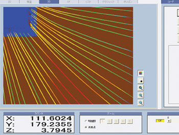
A loop height measurement tool detects the highest point of each loop of gold wire after bonding.
The confocal measuring head delivers low overall aberration — spherical aberration, in particular. Any spherical aberration would change the position of the concentrated light reflected through the objective lens. To minimize the problem, the Nipkow disk is arranged on the horizontal axis, which is in the same direction as the optical axis.
We also have developed a new approach to the Nipkow disk, using a pinhole with a diameter and position that make the height measurement datum plane correspond with the Nipkow disk plane. This results in high accuracy and flatness and prevents errors resulting from rotational issues.
Precisely measuring semiconductor packaging requires not only high accuracy, but also high speed. The most efficient way to obtain high-speed measurement is to maximize a wide field of view, accomplished with a variety of objective lenses that have a high numerical aperture (to 0.3).
Parallel processing enables high-speed measurement, but pipeline processing handles the image capture and the height measurement calculations. After the image is captured, the height measurement calculation finishes immediately. The next multimeasurement process begins and quickly produces the results.
The whole package
To move beyond the wafer, measuring the features of an integrated circuit package often requires a conventional vision system. Therefore, the confocal system includes a second optical path that has all the basic video measuring capabilities of edge detection, coordinate measuring and laser scanning. We separated the functions of bright-field edge detection and laser autofocus from confocal imaging, and users can switch between optical systems.

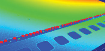
The confocal system has applications in the inspection of various features and packaging components used to produce 3-D architectures, including these gold bumps on a wafer-level chip-scale package. Courtesy of Association of Super-Advanced Electronics Technologies.
The objective lens is common for bright-field, laser autofocus and confocal imaging. Using these capabilities, 2-D (X-Y) and height (Z) measurements can be produced simultaneously. The system also includes a programmable teaching file that accelerates learning.
Semiconductor companies are producing a large assortment of 3-D architectures for semiconductor integration and packaging. Stacking strategies are being used frequently to save space on PC boards. Even stacking of die-to-wafer and wafer-to-wafer connections is under evaluation. This makes Z-axis height inspection for measurement of bumps, wires and other key features and packaging components critical to control and maximize process yields.
Meet the author
Michael Metzger is general manager of industrial microscopy and metrology at Nikon Instruments Inc. in Melville, N.Y.; e-mail: [email protected].