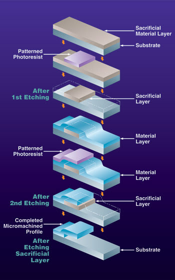
An overview of the surface micromachining process for MEMS device fabrication.
Melinda Rose, contributing editor, melinda.rose@laurin.com
A microelectromechanical system (MEMS) can be built either through bulk micromachining or surface micromachining techniques. In bulk micromachining (the oldest method of creating silicon-based MEMS), the microstructures are built inside the substrate, while surface micromachining, as the name implies, involves building the structures on top of the substrate. Bulk micromachining is a simple, inexpensive method used for creating MEMS with simple applications; more complicated applications require surface micromachining.
The electronics for most MEMS are fabricated through processes used to make integrated circuits (ICs), while the micromechanical parts are made by selectively etching away parts of the substrate or adding new structural layers. The base layer, or substrate, can be made of silicon or other materials, including plastics, metals, glass and diamond. As with ICs, MEMS structures are created using thin films of materials, which are patterned using photolithographic methods.

In surface micromachining, a MEMS is built by alternating layers (thin films) of structural material with “sacrificial” layers that later are removed to allow movement of the structural layers. The structural layers can be patterned by applying a mask. The completed MEMS typically ranges in size from 1 to 100 µm, or about the width of a human hair.
Various processes can be used to deposit the thin films. Thermal oxidation – oxidizing the surface in an oxygen-rich atmosphere – is a basic method, but the films have limited uses in MEMS.
In chemical vapor deposition (CVD), a silicon wafer or other substrate is placed in a chamber into which gases are pumped. The gases react and condense into a solid material on the substrate surface. Epitaxy, a method of CVD, involves the growth of a single crystal film on a single crystal substrate. The attraction of epitaxy is the ability to form relatively thick films (>100 µm).
Physical vapor deposition uses processes such as evaporation and sputtering to deposit thin metal layers. Electrodeposition, also known as electroplating, also is used to deposit metal films. In this method, electrically conductive materials are placed in a liquid solution and an electric current is applied.
Other deposition methods include evaporation, sputtering and casting.
Patterning is added through lithography techniques, usually by exposing a photosensitive material to a radiation source, such as light. The pattern of the radiation on the material is transferred to the exposed parts of the material.
Wet and dry etching processes are used to selectively remove parts of the various layers of the MEMS that are no longer needed. Wet etching involves immersing the material in a chemical solution, while dry etching comprises various methods for using reactive ions or an etching agent to remove material.