Line-scan cameras are indispensable for electric battery and semiconductor inspection.
JOEL WILLIAMS, ASSOCIATE EDITOR
In their most basic form, line-scan cameras have a single row of pixels. To capture an image, the object being imaged must be moving at a known speed. An encoder provides a feedback signal from a moving belt into the camera to tell it when the speed is increasing or decreasing. Image data is then sent from the camera via cable to a frame grabber, or directly to the computer’s local area network (LAN) input via network cable. Depending on the application, lighting requirements, which become more important at higher speeds, may also need to be considered.

As web speeds increase, so too does the importance of lighting. The Corona II family of lights provides high brightness and a variety of colors to facilitate various high-speed applications. Heat produced by high-intensity settings can be mitigated with water-cooling systems. Courtesy of Chromasens.
Despite the complexity of line-scan cameras, they hold significant advantages over area-scan cameras for certain applications. For one, they’re able to provide higher-resolution images, which are built one line at a time.
“It’s one line at a high resolution — much higher than you can get with an area scan,” said Jeremy Jowers, director of sales and business development at Chromasens.
Line-scan imaging is most useful for inspection applications in which an object is moving along a conveyor belt, such as during printing, foil, paper, packaging, and postal inspection, according to JAI’s director of product management, Paritosh Prayagi.
Many of these applications are classified as web inspection, or inspection of a moving 2D object. Inspection is often performed by contact image sensors, so-called for their extreme proximity — by a distance of a matter of millimeters — to the object they are inspecting.
Despite the fact that such applications are among the oldest for line-scan technology, they are also among the most demanding when it comes to speed. With the move toward Industry 4.0, manufacturers are increasingly focused on acquiring information from line-scan cameras faster and more
efficiently. Data rates between line-scan and area-scan cameras are neck and neck, but when it comes to speed, line-scan technology holds a clear advantage.
“For area-scan cameras, even at very high frame rates you can still have some blurring with fast moving objects,” said Dale Deering, senior director of business development at Teledyne DALSA. For an area-scan camera to capture an object without blur, the object often must be either slowed down or stopped.
“Speed is one of the factors where things have been moving forward,” Prayagi said. Cameras can operate at 400,000 lines per second. “This is
really, really, high speed. And it’s at least 20 to 30× faster than the fastest area-scan sensors available.”
To accommodate these speeds, advancements on the interface side have included updated machine vision standards such as 50 GigE and 100 GigE ethernet connectivity, Prayagi said. “But you still have a bottleneck on the processing side because, even if you acquire at those kinds of line rates, there is a limitation on what can be processed in real time.”
Much of this limitation depends on the processing architecture, including issues such as GPU versus CPU, how the load is managed on the computers, and how the parallel processing itself is executed, Prayagi said.
Creative preprocessing techniques that occur within the camera itself, where only the essential data is fed to the processing unit, can accommodate limitations in processing power. Other methods include parallel processing, which splits the information between multiple processing units, Deering said.
This can be accomplished by using Dual 10 GigE, an interface that uses two network cables to bring in more information at once.
“The drawback is that if you were to do this yourself, you would have a problem — especially in Windows, where the operating system will try to manage the network adapter while you’re trying to run a real-time camera over it,” Jowers said. Certain protocols from the operating system can slow the speed of information being transmitted, which can cause problems with real-time applications.
“That’s why GigE is often derated from 1 GB per second to 700 MB per second, depending on the network configuration,” he said.
To solve this issue, Chromasens employs a special driver to prevent interruptions from the operating system, thereby enabling camera data to be streamed directly into the computer using readily available 10 GigE or dual 10 GigE networks. This can reduce costs by eliminating the need for
specialized frame grabbers.
In addition to parallel processing, innovations in machine vision, such as integrated AI, are starting to make their way over to line-scan technology.
These capabilities allow the camera to extract the relevant information and then send it to the processor. Without extraneous information, real-time processing remains achievable.
In-camera processing
Teledyne’s Deering provided the example of a process in which particulate matter is being released. Customers may want to be able to identify a particular type of material so that they can identify where in the process the particulate is being released, and they can then perform the relevant maintenance. An application such as this would require multispectral or even hyperspectral imaging, which produces a great deal more data. In-camera and edge processing techniques can perform simple data reduction to facilitate real-time processing.

The potential defects in semiconductor wafers can be incredibly small. Line-scan cameras detect defects as small as 8 μm.
Courtesy of Stock.com/kynny.
A dual camera setup provides a broader view at shorter working distances. The cameras must be carefully aligned using xyz stages. Software advancements have made this process considerably easier. Courtesy of Chromasens.

An imaging system designed for semiconductor wafer inspection. The system uses two monochrome cameras and a lighting system to provide bright- and dark-field illumination for accurate detection of nondirectional scratches and other defects.
Courtesy of Chromasens.
Using in-camera processing, the customer could isolate the spectral range of the particulate matter in
question to be sent to the processing unit so that it could be identified in real time.
This capability stems from the shift in the industry that occurred about five to 10 years ago — the move from CCD to CMOS. With the CMOS image sensors available today, many image corrections can be performed within the camera itself, thanks to the sensor’s digital signal (as opposed to CCD’s analog one). CMOS also enables higher-speed imaging and allows much greater pixel density.
“As devices continue to get faster and smaller and cheaper, you’re able to do a lot more within the camera than you could in the past,” Deering said. “In the past, it was best to do the processing in the host, but today some of that processing can be done right in the camera.”
Lower-cost devices are growing not only in their processing power but also in terms of the features they can deliver for customers. Teledyne’s Linea 2
family of line-scan cameras is focused on size, weight, power, and cost (SWaP-C).
“This technology is based on a quadlinear architecture, and we have been sampling RGBN, or RGB plus near-infrared,” Deering said. “We do have that on some of our upper-end products like the Linea ML, but this is the first time we’re implementing it on value-oriented products.”
The near-infrared (NIR) channel
allows customers to conduct bright-field imaging with the RGB portion and dark-field with the NIR channel during the same pass, simply by adding an NIR LED strip.
Along the same lines, time delay
integration line-scan cameras utilize more lines to enable images to be taken at various light intensities, to gain a better picture of low-contrast features and defects, for example.
More light
As with most forms of imaging, at higher speeds, light becomes more important. Shooting a high-speed subject with a digital camera might boost the shutter speed and compensate for the loss of light by using a large-aperture lens and a higher ISO (light sensitivity) setting. With a line-scan camera, the faster speed simply requires more light.
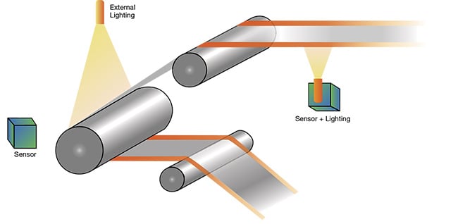
A typical setup for a roll-to-roll application. Because these targets move quickly, they must be properly illuminated, and they must be imaged on both sides to ensure that quality standards are met. Courtesy of Teledyne.

Objects such as the ball grid arrays used for integrated circuits must be imaged in 3D to ensure height uniformity. Stereoscopic line-scan cameras are used to tackle this challenge. Courtesy of Chromasens.
At short working distances, this increase can be achieved by implementing mirrors to confine the light to the imaging area. Lenses are often used to concentrate the light into a single uniform beam across the line.
Multiple lights can be used to facilitate features such as time delay integration and multispectral imaging.
It should be noted that having a state-of-the-art lighting setup may not be vitally important.
“If you can get away with a $100 light that works in an aquarium, I’m not trying to change it,” Jowers said.
Most line-scan cameras today are equipped to deal with some variability in light uniformity. But for some applications in which color is vital, having a good light is imperative to ensure image fidelity at all imaging points in the production line.
In 3D applications, which are achieved stereoscopically, lighting is important to ensure that no areas are shadowed.
“In 3D, it really helps to optimize the lighting. Sometimes a focused beam is best. In other cases, a diffused light, like the Chromasens tube light, or
coaxial is optimal,” Jowers said.
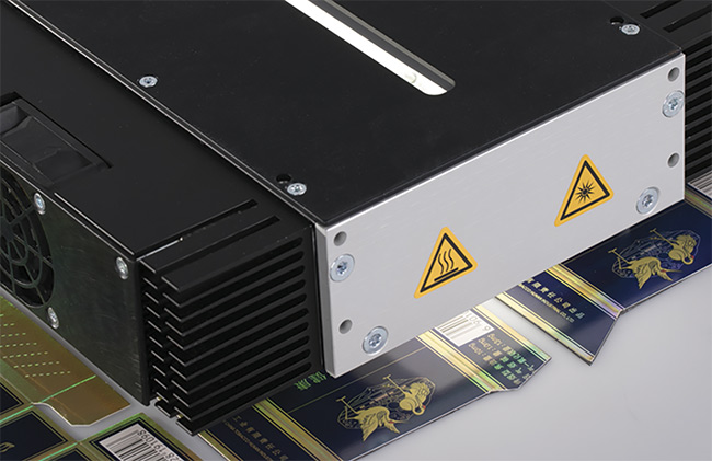
Contact image sensors, one of the oldest types of line-scan cameras, provide high-speed inspection of flat targets, such as cardboard packaging. Courtesy of Chromasens.
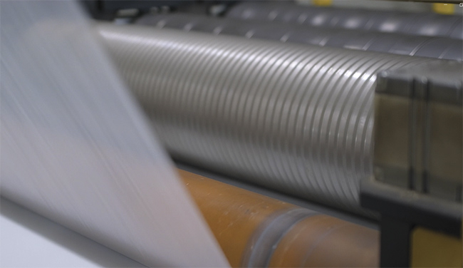
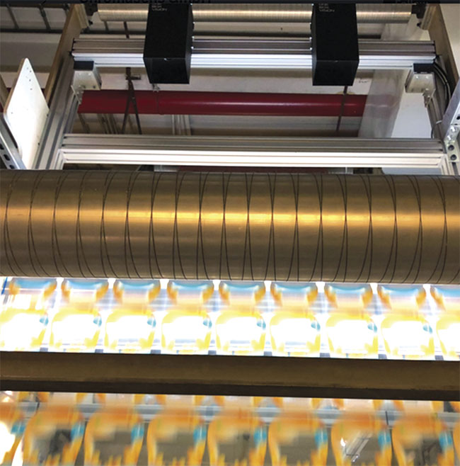
For roll-to-roll processes, line-scan cameras are best implemented at points where the film is smoothest, such as where it lies against a roller. Courtesy of JAI.
One unique application for 3D line-scan imaging is road inspection.
“You put an encoder on the vehicle’s wheel to inform the camera of the surface speed. You have to have two lights and the 3DPIXA camera in the middle — really, it’s two cameras focused on the same field of view,” Jowers said. “And then inside the vehicle it looks like an FBI surveillance van. You’ve got a server in there along with other electronics. They have a GPS system that will marry the capture location with the image so you know where the defects are present.”
The vehicle can travel up to 60 mph while imaging the roadway, with cracks and defects visible down to a millimeter.
CHIPS Act spurs demand
With the CHIPS Act and the European equivalents signed into law, a large number of semiconductor fabs are slated for construction. Along the same lines, the move toward electric vehicles, spurred by climate change mitigation efforts, is driving up demand for lithium batteries. Those battery manufacturing facilities are motivated to get up and running quickly. In both manufacturing contexts, line-scan technology is an integral inspection tool.
“That sets up an opportunity,” principal technology analyst for IDTechEx, Matthew Dyson, said. “With semiconductor manufacturing and other bits of manufacturing, we have an opportunity to incorporate cameras for quality control, and perhaps more motivation to do it with SWIR [short-wavelength infrared] because it can see through silicon.”
When it comes to battery inspection
and semiconductors alike, high resolution is key. The potential defects are very small, JAI’s Prayagi said, which means the cameras imaging them need to be very high resolution.
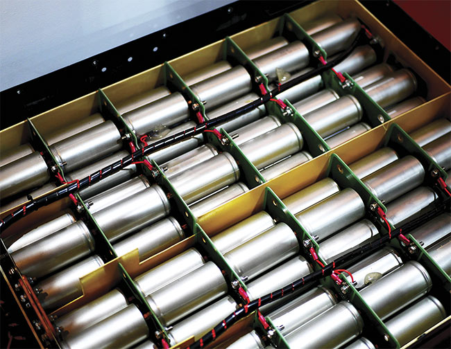
Each cell of a battery for electric vehicles contains rolls of carbon-coated films that must be inspected for quality assurance by line-scan cameras. Courtesy of iStock.com/Supersmario.
“The challenge is when you go expand on the resolution, you are basically reducing your pixel size,” he said. “It’s also a sensitivity issue. How sensitive is your camera to small changes? How is the full-well capacity on the sensor, or the quantum efficiency, the noise levels?”
With smaller pixels comes a greater need for light, which also plays into the need for a high full-well capacity. This capacity involves the amount of signal electrons that can be collected in the pixel, Deering said. Even with adequate lighting, if the pixels are overwhelmed with signal electrons, the image becomes saturated, which compromises quality. A higher full-well capacity grants greater potential for a high signal-to-noise ratio.
In battery inspection, many of the processes are so-called roll-to-roll, a classic line-scan application in which a roll of, say, aluminum foil is unrolled, inspected, and then returned to its rolled form.
“You inspect the coating thickness, you inspect the alignment of the structure on the film, you look at both sides of the film for scratches or defects, and you also look for contamination,” Prayagi said, referring to the battery manufacturing process.
This process requires a great deal of speed, he said. The process requires a high-resolution system, so depth of field can become an issue. With higher-resolution cameras, the depth of field is further from the camera itself. Even small movements can alter the image’s integrity.
“With a lot of cameras, you can get away with some movement in the object because your resolution is fairly low, your depth of focus is really high, and it’s not that big of an issue,” Chromasens’ Jowers said. “With electric vehicle battery inspection, it’s very high resolution which gives you a very low depth of focus, which means you need to have a very controlled target.”
In high-resolution roll-to-roll processes, movement is handled by introducing a roller.
Picture a VHS tape. The film goes from one spool to the other and is read at the center. To get from one side to the other, the film has to move at two fairly extreme angles. At those points, rollers are introduced that spin with the motion of the film, allowing the player to produce a smooth image and clean audio.
At the roller, the film is taut and perfectly flat (provided that the roller itself is). This is where the image is taken. Because the materials being inspected are of a uniform color, monochrome is the camera of choice.

While most line-scan cameras are equipped to deal with some motion in the target, unstable objects such as potatoes can produce more movement than the camera can account for. A prism-based camera, while more expensive, handles the irregular motion more effectively.
Courtesy of JAI.
Vital to the efficacy of this inspection process is the geometry of the setup itself.
“Otherwise, you end up with a lot of reflections and not seeing the defect,” Prayagi said.
In semiconductor inspection, the bigger challenge is the size of the defects. “It could be as small as a dust particle, so I think the big challenge there is on the resolution side, but also to have extremely good optics in order to identify a dust particle that is a couple nanometers large.”
Prayagi said he does not expect an immediate boom in demand for line-scan cameras. Semiconductor manufacturing and demand has a cycle of about seven to eight years. We are currently entering the low phase.
IDTechEx predicts the number of line-scan cameras sold to increase by about 10% per year, while growth rates for SWIR imaging cameras and the associated software packages are expected to be higher.
Prism-Based Cameras
One of the newer entrants to the line-scan landscape is the prism-based camera. At present, one of the only companies that offers such a device is JAI. This type of camera is useful when the speed of the object is uncertain. JAI’s director of product management, Paritosh Prayagi, provided the example of inspecting potatoes.
“The objects are not stable, [and] they’re also vibrating, moving, rotating, and so on,” he said. “When you have these objects moving at different speeds, that’s when prism technology is very helpful. Because, unlike the traditional color line-scan cameras, which are the trilinear cameras, we don’t have any kind of a line gap on the sensors.”
A traditional trilinear camera focuses on separate lines for red, green, and blue, and in between them are gaps, Prayagi said.
“If the object speed is changing too frequently, then the RGB lines are not able to overlap onto each other at the right time,” Prayagi said. “If there’s a signal frequency mismatch, this can lead to something called a halo effect.”
In an RGB prism camera, the light is sent to three separate sensors simultaneously,
eliminating the possibility of a color mismatch that can occur in a trilinear camera. However, with the increased number of sensors — and, of course, the prism itself — comes an increased cost.
“It’s not applicable for each and every line-scan application, but an application where the value is there, I think the cost doesn’t play a big role,” Prayagi said.
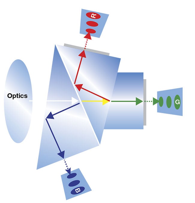
The separation of light inside a prism block. Courtesy of JAI.
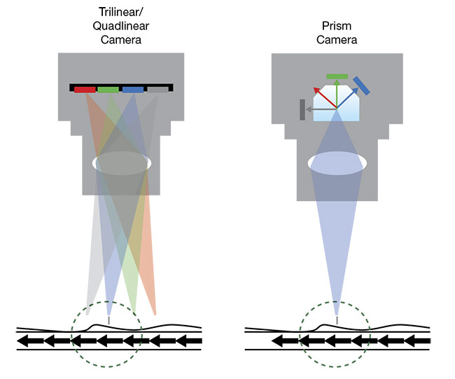
The individual lines in a trilinear camera are separated from each other by a line gap that can be one pixel or smaller, creating a slight optical shift for each of the colors. Courtesy of JAI.
|