From lighting and television screens to displays, smart devices and light-absorbing windows, OLEDs are turning up in an increasing number of applications. Many companies are taking advantage of the opportunities they provide, working on more efficient, affordable solutions to allow greater manufacturing output.
That glowing screen in the palm of your hand might foretell the future. It’s not some new app, but the screen itself. OLEDs — organic light-emitting diodes — have muscled their way into mobile applications and are now found on many devices.
“You’ve got something like 400 to 500 million displays, at least, that have been manufactured to date worldwide,” said Mike Hack. “So it’s been very successful in mobile.”
Hack is a vice president at Universal Display Corp. of Ewing, N.J. The company invents and develops phosphorescent OLED technologies and materials for the display and lighting industries.
Devices and films that absorb light and emit electrons, the reverse of what’s done in a display or lighting, are another possible application of organic materials. Windows covered with a film could then generate power while letting in light. Also, the walls of a building could produce electricity. Similar to what’s done with silicon photovoltaics, existing structures could be retrofitted.
At present, displays have attracted perhaps the most attention, thanks to a large market where high-performing devices command a premium. However, advances made in displays could benefit lighting and light-absorbing applications.
As for OLEDs, Hack noted that they are showing up in televisions and general lighting. In either, the ability of organics to operate on flexible substrates could allow novel capabilities.

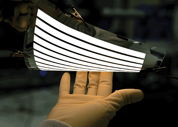
OLEDs can power flexible lighting and displays. Photo courtesy of Universal Display Corp.
Researchers are working on a number of areas to help OLEDs and other organic devices achieve a bright future. For instance, the organic molecules used cannot survive prolonged exposure to air or water and so must be protected through encapsulation, which is a challenge when using porous, flexible substrates. While current techniques work, companies are researching and developing better and cheaper solutions with fewer process steps; this will allow greater manufacturing throughput, Hack said.
Another issue is efficiency, an area where even better performance is possible than what can be achieved with a fluorescent approach, which is about 25 percent efficient, according to Hack. “Our phosphorescent OLED technology converts virtually 100 percent of the electrical energy into light.”
A third challenge involves cost. OLED displays are made using a fine metal mask to create the pixel pattern. In this approach, a thin sheet of metal with holes in it is placed over the substrate, and the organic molecules travel through the holes before ending up on the substrate.

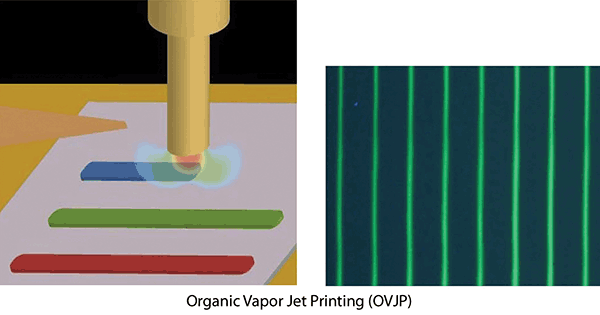
The organic molecules in an OLED can be put down using organic vapor or inkjet printing, enabling fine features and high pixel densities to be created economically across large displays. Photo courtesy of Universal Display Corp.
That is cost-effective for small displays, which helps explain why OLEDs have done so well in mobile applications. When the same technology is scaled up for a large display or television, however, drawbacks appear. It becomes difficult to make the masks and to maintain the proper tolerance. Also, during processing, the masks have to be cleaned periodically. What’s more, the mask must be precisely positioned from one pass to another so that the different colors found in each pixel properly align to each other. Partly as a result of such factors, today a large OLED TV can be many times the cost of a similarly sized LCD TV.
One solution is to take advantage of the fact that the organic molecules are in solution. That makes it possible to employ a different approach. An example comes from DuPont Displays, part of the Wilmington, Del.-based chemical company. DuPont Displays recently announced it had teamed up with inkjet equipment manufacturer Kateeva of Newark, Calif., to develop optimized inks, equipment and processes to further advance inkjet printing technology for OLED devices.
Avi Avula, global business director for OLEDs at DuPont, explained the advantage of a printed approach over the current method by referencing the painting of a table. With an evaporative technique, such as is used in current OLED display manufacturing, paint goes everywhere.
“But if you use solution-printed technology, you’re only putting the materials on the table. Basically, you’re painting the table rather than spray painting the whole room,” Avula said.
In addition to saving material, the printed approach makes the manufacturing process simpler. There is no need to produce, maintain or clean a shadow mask. Another manufacturing simplification is that there’s no mask alignment required.
A different technique, one based on patterning, has been a focus at imec. The Leuven, Belgium-based nanoelectronics research institute recently announced it and Japan’s Fujifilm Corp. had demonstrated successful OLED patterning using photoresist and photolithography. Each pixel consisted of red-green-blue, the three components needed for a full color display. As for the pixel density, this was about as good as that found on high-end commercial phones, where devices currently run about 500 pixels-per-inch (PPI).

“We demonstrated 20-μ pitch which translates to something like 640 PPI resolution. At the same time, we know the resist is capable of going to submicron resolution,” said Pawel Malinowski, a senior researcher at imec.
This processing is done in a standard cleanroom and with regular tooling. That means the organic molecules are exposed, albeit briefly, to the degrading effects of the ambient atmosphere. The researchers examined the impact of this on OLED performance and longevity, discovering that there was an effect. For instance, the performance margin might be cut by a third. That issue is being addressed through ongoing research and development, Malinowski said.
He added that an advantage of the imec/Fujifilm approach is that it uses tools widely used today, making the method more interesting and valuable to manufacturers.
OLEDs can be printed or patterned on flexible substrates, something impossible to do with other lighting and display technologies. This opens up such possibilities as displays that can be rolled up, flattened for use and then rolled up again. It also makes possible the creation of curved lighting that, for instance, hugs a wall and travels around a corner.
Displays and, to a lesser extent, lighting have attracted the bulk of interest in OLEDs. However, there are other places where the technology or something closely related could show up as well. As mentioned, organic molecules similar to those developed for OLEDs can do the reverse of emitting light, and therefore can be used in a sensor or to make power.
Some of the work being done on OLEDs could benefit such absorbing devices. For instance, the patterning of organic molecules enables different colored OLEDs to be integrated next into other devices, with everything fitting together in a small area due to the tight pitch. The same technology could also prove useful in an absorption scenario for a photodetector or imager.
“With such solutions, you can think of having neighboring pixels made of different materials, and so sensitive to other colors. Similarly to OLEDs, you can think of substituting the color filter array by a patterned active layer for absorbing different colors,” Malinowski said.
For power production, on the other hand, patterning or printing would prove much less useful. The demand is not to have individual pixel responses but rather to get performance out of an entire array. However, this doesn’t mean that the organic molecule research and development work aimed at OLEDs won’t benefit such applications.
“We have had good evaluations of some of our charge transport materials in [organic photovoltaic] devices by several customers. We are confident our materials work well in that application and we are ready if the technology is commercialized,” said DuPont’s Avula.

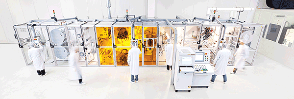
Heliatek makes organic solar films in a roll-to-roll process using vacuum deposition at low temperatures. Photo courtesy of Heliatek.
An example of what might be possible can be seen in Singapore, where Dresden, Germany-based Heliatek GmbH’s organic photovoltaic films are being used in a building on various materials and locations. The film is being put down within and on glass, on steel, and on curved polycarbonate. Several versions of the company’s flagship film will be used, ranging from full power harvesting opaque to those with transparency levels of 15 and 30 percent. There also will be some of different colors.
One recipe of chemicals and organic molecules found in power-producing films and OLEDs comes from technology developed by Novaled GmbH of Dresden, Germany. Novaled researches, develops and commercializes technologies and materials that enhance the performance of OLEDs and other organic electronics.
The improvements being investigated and developed involve conductivity, power efficiency, brightness, lifetime, and other basic material and device properties. The company also works on enhancing device and material manufacturing processes, according to Witali Muth, a senior sales manager at Novaled.
The benefits that result from these and other innovations by those in the industry could soon be in hand — perhaps quite literally. “Smartphones can run longer on one battery charge when OLED displays work more efficiently, or under harsh conditions when the low-temperature performance of OLED displays is better,” Muth said.