Aaron J. Hand
As the semiconductor industry struggles to expand optical lithography's capabilities and decide on the next-generation tool, one research group has come up with an alternative. A team at the IBM Zurich Research Laboratory has developed a relatively simple optical technique that prints features measuring less than half the wavelength of the light source. And it does so without using complex and expensive focusing optics.

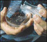
Light stamps are formed by molding them on a silicon master. Courtesy of IBM Zurich Research Laboratory.
The technique uses a "light stamp" that is placed directly on the wafer. Unlike traditional contact lithography, which uses chrome-on-glass masks, the new method uses a rubbery mask that makes uniform contact with the wafer.
Protrusions on the stamp form the pattern to be printed. When the light hits the stamp, it shifts to a shorter wavelength and is guided into the substrate by the protrusions and blocked or reflected in the recessed areas. The light is focused in the protrusions, and the close contact between the stamp and resist -- whose refractive indexes match -- avoids scattering.
The group has printed linewidths as narrow as 100 nm with a 248-nm light source, and expects to be able to take that further. The researchers have not experimented with 193- or 157-nm lasers partly because the stamp material they are using absorbs too much at those wavelengths, according to Bruno Michel, one of the researchers on the project. But it may not even be necessary to use shorter-wavelength light sources, he pointed out.
"I believe it is not so important to reduce the vacuum wavelength of the exposure light by a factor of 1.3 to 1.6, but to increase the refractive index of the stamp material instead," he said. "This, for example, can potentially reduce the minimal feature size by a similar factor. Other optical approaches might allow a further reduction of the minimal feature size so that smaller vacuum wavelengths than 248 nm are not necessary."
Defect potential
The researchers are beginning to trace and understand defects in the resist, which can be induced by dust particles or small defects on the stamp, Michel said, adding, "Standing waves in the protrusions of the stamp can cause interference patterns in the exposure and sometimes lead to defects in the exposed resist pattern." But IBM's system does not seem to cause defects or contamination on the wafer, he said.
Such contact lithography methods have the potential to compete with optical lithography or next-generation methods, Michel said. Unlike next-generation techniques, the light stamps can use resists used in optical lithography, avoiding large investments in this area.
The light stamp method is early in its development. "We are sure, however, that the complexity of this method is much lower than that of any of the new lithographies," Michel said.
IBM does not yet have plans to use the light stamp method in high-volume chip production, but might first use the technique for niche applications, Michel said.
