Lens-Free Imaging for Large-Surface Industrial Inspection
Jan Provoost, imec
With micro- and nanofabrication surging, there is a growing need for cameras that can automatically monitor large surfaces for microscopic details. Scanning setups with conventional microscopes are sometimes used, but they are too slow and bulky for many applications. Lens-free holographic imaging may offer a solution – it allows a lighter setup, is faster and examines a much larger surface.
Lens-free imaging applications include industrial and medical uses. Photonic integration allows the light source and the imaging chip to be collapsed into a form factor that will allow automated inspection in even the most demanding situations.
A microscope without lenses
Lens-free imaging is based on holography. Dennis Gabor first formulated the principle in the late 1940s, earning him the Nobel Prize for physics in 1971. He proposed using a photographic plate to capture the interference pattern between the light that illuminates an object and the light that diffracts off an object. In this hologram, all the information needed to reconstruct a perfect image of the object, including depth information, is available.
In recent years, with the advent of sufficiently powerful CCD and CMOS imagers, Gabor’s photographic plates could be replaced with a fast, high-resolution digital image sensor. At the same time, computers have evolved to the extent that a high-end computing cluster is no longer required for image processing within a reasonable time frame. It has become practically feasible to convert the captured holograms into digital images by calculation. These digital images then can be further processed for detecting microscopic anomalies, inspecting form factors, counting microscopic objects and more.
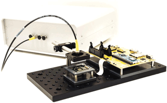
The first lens-free microscopes built by imec researchers were based on a simple premise: Take a coherent light source (e.g., a laser) and shine it on the sample. Then, on a digital image sensor, record the interference between the light that has interacted with the object and a reference beam (i.e., the original light beam). Finally, reconstruct the image for visualization and information extraction. This setup requires only a light source, an image sensor and a powerful processor to compute the images in near real time. Moreover, the image capturing and interpretation process is completely digital, eliminating any need for manual intervention or mechanical calibration and focusing.

Markets for imec’s prototype lens-free microscope include the industrial and biomedical industries.
This basic setup enables microscopes that can either see through transparent samples or look at reflecting, nontransparent surfaces.
With a transparent sample, the light passes through and then interferes with the reference beam. This design proves especially useful for applications in the biomedical domain, as it can inspect transparent living samples without the need for staining. An example application in development is the automated monitoring of stem cell colony growth. For such applications, this solution proves a good alternative for phase-contrast microscopes, equaling the resolution but allowing a much larger field of view..
For nontransparent surfaces, a suitable solution is reflective holography, where the hologram is made from the interference of the reference beam with the light that reflects off an object. This mode can be used for industrial inspection of large surfaces for micrometer-sized features, which may include looking for anomalies and contamination on solar cells, displays or ultraclean surfaces, or counting microstructures or inspecting their forms (e.g., wafers, micro-PCBs)..
A large, scalable field of view.
The biggest difference in lens-free systems versus traditional microscopes is that the field of view doesn’t depend on the resolution but on the size of the image sensor. For our first microscopes, we selected a state-of-the-art monochrome 10-MP imager with 1.67-μm pixel pitch and a fiber optic coherent light source. With this setup, we obtained a resolution of 1.23 µm and a field of view of about 30 mm² ¬– orders of magnitude larger than what is possible with traditional microscopes at this resolution. For large-surface inspection, this means less mechanical movement and image stitching.
Additionally, the lens-free hardware is scalable. The image sensors can be placed next to each other with no gaps. As a result, it is fairly simple to extend the field of view in one dimension. This would limit the scanning needed to only one dimension.
In some setups, users need to inspect the way features change over time. As these changes may be subtle, inspection requires a high imaging speed. This speed, of course, depends on the speed of the image sensor, as well as on the speed with which pictures can be digitally computed, either in real time or with postprocessing. For high-speed setups, the computation and hardware can be optimized using a combination of GPUs and a CPU. By using this setup along with postprocessing, imaging speeds of almost 300 frames per second were achieved, with higher speeds possible.
The resolution of the lens-free microscope is a function of the pixel size of digital imaging chips. With a robust market for such chips, and with production quantity of these imagers exceeding 1 billion units per year, the technology is quickly improving. Imec reached a record 870-nm resolution on a standard USAF-1951 test target using a commercially available Toshiba image sensor with a 1.12-µm pixel size.

Stem cells seen through a phase-contrast microscope (left) and through imec’s lens-free microscope (right).
Photonic integration of light source
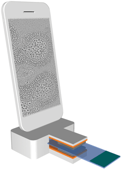
Lens-free microscopes could become real game-changers if they could be fully integrated within a chip package – a package not much larger than today’s standard image sensors found in devices like smartphones. In that case, microscope functionality could be built into virtually anything. And on production lines, it could achieve ultrahigh throughput, inspect very restricted spaces, and allow for scaled solutions by combining arrays of chips.

A miniaturized, fully integrated microscope-on-a-chip used as a mobile phone extension.
Although much simpler and smaller than traditional microscopes, the lens-free prototype with large field of view still takes up a considerable amount of space. The main reason is that the coherent light source has to be positioned perpendicular to the image sensor as well as to the inspected surface or sample, and at some distance. To shrink the microscope, this third dimension has to be all but eliminated.
Waveguide technology using silicon photonics – a technology already successfully introduced into sensor and communication applications – can be used to replace the light source. An obvious advantage of a waveguide solution in silicon is that it can be fabricated in large quantities for a low price per unit. Moreover, waveguide chips are mechanically and thermally robust and stable. For this application, however, the major advantage is that these chips have a very compact 3-D profile. The silicon nitride (SiN) waveguide processed on top of a substrate is not higher than one micron.
The main challenge was to design these waveguides so that they deliver light to the microscope with the desired characteristics. For applications with a large field of view, this means quasiplanar, coherent waveforms. The microsized solution involves using a fractal layout of phase-matched waveguides designed to generate multiple light sources that create a quasiplanar illumination wavefront over an area of a few square millimeters.
With this solution, the waveguide chip can be placed within a few millimeters of the sample. The prototype using this technology reaches an imaging resolution of 870 nm by using an image sensor with a 1.12-µm pixel pitch and has a field of view of 12.2 mm2.
Meet the author
Jan Provoost is a science editor at imec in Leuven, Belgium; email: [email protected].
/Buyers_Guide/Imec/c22187