Haihua Tang1, Yunfei Liu1, Shuang Liu1, DeJun Chen1, Yong Liu1, zhiyong Zhong2
1University of Electronic Science and Technology of China, School of Optoelectronic Information, Chengdu, China
2University of Electronic Science and Technology of China, State Key Laboratory of Electronic Thin Films and Integrated Devices, Chengdu, China
A double absorbing layer based on amorphous silicon thin film is promising for solar cells because it considerably enhances the utilization of sunlight.
Other potential applications can be found in the field of IR detection.
Over the past few decades, hydrogenated amorphous silicon (a-Si:H) thin film has been widely studied because of its potential use in a wide variety of devices, such as photodetectors, large-area displays and xerographic applications.1-6
It was considered an especially strong candidate for preparing solar cells because of its remarkable advantages: low production cost, large-scale deposition and low-temperature production.7-9
However, as a single absorbing layer, a-Si:H thin film can absorb only certain wavelengths of the sunlight spectrum.
In addition, as a single absorbing layer of solar cells, it can only absorb part of the visible light spectrum.10 The narrow absorption spectrum of a single-junction solar cell limits the use of the entire solar spectrum.11 Stacking multiple photoactive materials with different bandgaps is a possible solution to enhance the conversion efficiency of solar cells.12-13 The solar spectrum will be better used with the aforementioned solution, resulting in enhanced absorption efficiency of sunlight.
In the following study, a-Si:H thin film and microcrystalline silicon (μc-Si:H) thin film were selected as two materials with different optical bandgaps to achieve this solution. Although a number of different techniques are commonly employed in the deposition of a-Si:H thin film, the main method is plasma-enhanced chemical vapor deposition (PECVD).14-15 We chose the PECVD technique because it provides high deposition rates for a-Si:H thin film. Furthermore, it is easier to control and requires low cost. The μc-Si:H thin film can be produced by scanning the a-Si:H thin film with a nanosecond laser at 532 nm in an atmosphere of sulfur hexafluoride.
In this work, a double absorbing layer consisting of a-Si:H/μc-Si:H was prepared using the radio frequency (RF) PECVD technique and a nanosecond-laser-scanning method. The feasibility of the double absorbing layer scheme was analyzed using computer simulation software, and we compared the difference in absorption characteristics between the a-Si:H/μc-Si:H layer and the a-Si:H layer.
Experiment
The hydrogenated a-Si:H thin films were deposited on a glass substrate using a 13.56-MHz RF-PECVD system. Silane (SiH4) was used as a working gas, and the flow rate of SiH4 was 40 standard cubic centimeters per minute. Deposition pressure, substrate temperature and radio frequency were maintained at 80 Pa, 300 °C and 20 W, respectively.
After deposition, the samples were scanned with the 532-nm nanosecond laser in an atmosphere of sulfur hexafluoride (SF6) to achieve the μc-Si:H thin film layer.
The double absorbing layer of a-Si:H/μc-Si:H was obtained by depositing an a-Si:H layer onto the μc-Si:H layer with the aforementioned process conditions.
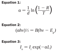
The feasibility of the double absorbing layer scheme was analyzed by the computer simulation software. Transmission and reflection spectroscopy of the a-Si:H, μc-Si:H and a-Si:H/μc-Si:H thin films was performed using an ultraviolet-visible (UV) spectrophotometer. The thin films’ thicknesses were detected using a fiber optic spectrometer, and the absorption coefficient of film was calculated according to Equation 116, where α is the absorption coefficient, and d, R and T are the thickness, reflectivity and transmittivity of the films, respectively.
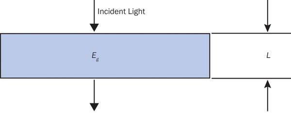
Figure 1. The structure of the single absorbing layer.
Simulations of single and double absorbing layer
Simulation software analyzed the spectral absorption’s characteristics of the single absorbing layer and double absorbing layers. The relationship between absorption intensity and wavelength was described by the Tauc plot17 and Lambert’s law18 (see Equations 2 and 3), where h is Planck’s constant, Eg is the optic bandgap, ν is the radiation frequency, α is the absorption coefficient, B is slope, Ii is incident intensity, Io is output light (also known as transmission light) intensity, and L is the thickness of thin film.
Figure 1 shows the model of the single absorbing layer. Specific parameters were set as follows: The film thickness was maintained at 0.7 μm. The values of the optic bandgap were set by 2.4 eV, 2 eV, 1.8 eV and 1.6 eV, respectively. A maximum relative spectral response of 1 was defined.
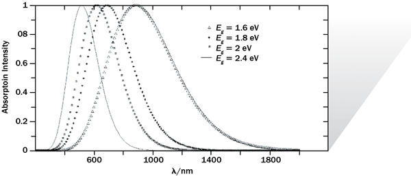
Figure 2. A simulation of the single absorbing layer with different bandgaps.
The simulation results of the single absorbing layer with different bandgap values are depicted in Figure 2. As the results show, the wavelengths at absorption intensity peak decrease with the increase of the optical bandgap. This indicates that the materials with a larger optical bandgap absorb the highly energetic lightwaves. The full width at half maximum (FWHM) spectral response increases from 260 to 500 nm with the decrease of the optical bandgap – i.e., the spectral absorption’s range of the film becomes larger with the decrease of the optical bandgap.
The double absorbing layer model is shown in Figure 3; it has a different bandgap at each layer: Eg1 and Eg2. Specific parameters were set as follows: For the purpose of comparison with a single absorbing layer, the total thickness of the film was 0.7 μm. The thickness was 0.4 μm when Eg2 was 2.2 eV, and the thickness was 0.3 μm when Eg1 was 1.6 eV. The relative absorption peak was 1.
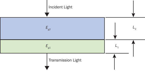
Figure 3. The structure of the double absorbing layer.
Figure 4 depicts the spectral-response simulation result of the double absorbing layer. It can be obtained from the simulated result that high-energy lightwaves will be absorbed by film L2, where the relative absorption peak is 0.8. In contrast, low-energy lightwaves will be absorbed by the film LL1. The solid line in Figure 4 is the envelope of total absorption – i.e., the absorption of the double absorbing layer, where the relative absorption peak is 1.2. The relative absorption peak of the single layer at the value of 2.2 eV (film L2) declines compared with the structure of the single absorbing layer. The reason for this is that the thickness of the film is less than the thickness in the single-layer model, resulting in insufficient light absorption. The absorption peak of the single absorbing layer (film L1) is 1, and the FWHM spectral response of film L1 is about 500 nm, while the absorption peak of the double absorbing layer is 1.2, and its FWHM of spectral response is 600 nm. This result gives a conclusion that the absorption peak and range of spectral response are improved obviously in the double-layer film with different bandgaps.
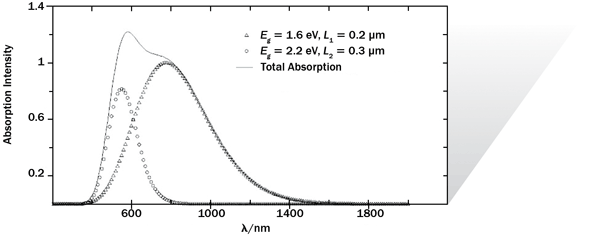
Figure 4. A simulation of the single absorbing layer and the double absorbing layer.
Experimental characterization
Figure 5 displays the absorption characteristic of the single absorbing layer (a-Si:H) and the double absorbing layer (a-Si:H/μc-Si:H). To achieve the values of the absorption coefficient (α) for the a-Si:H layer and the a-Si:H/μc-Si:H multilayer, two sets of results were obtained using the analysis based on Equation 1.
In the case of the a-Si:H layer, the result suggests that the single absorbing layer shows relevant spectral-absorption features in the entire visible region and part of the UV region (300 to 800 nm), with no absorption in the near-infrared (NIR) region. As shown, the peak of the absorption coefficient is located in the range of 300 to 500 nm, which can be up to six orders of magnitude. The absorption coefficient decreases significantly after 500 nm until it arrives to zero at 800 nm.
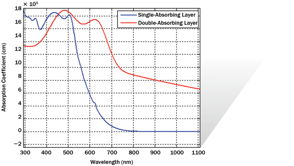
Figure 5. The absorption coefficient curve of the single absorbing layer and the double absorbing layer.
In contrast, the a-Si:H/μc-Si:H multilayer not only shows the remarkable spectral absorption features in the visible and part of the UV zone, but also has an obvious absorption in the NIR region (800 to 1100 nm). The absorption coefficient of the double absorbing layer is larger than that of the single absorbing layer over the entire measurement spectral range, except at 300 to 450 nm. The specific area will not affect the overall trend. It may also be noted that the a-Si:H/μc-Si:H multilayer shows a significant absorption characteristic in the NIR region; the absorption coefficient in this region can reach up to three orders of magnitude.
The results illustrate the double-absorption layer’s superior spectral absorption capacity, compared to the single absorption layer. The aforementioned simulation results can be used to explain this experimental conclusion. Because the a-Si:H has a wider optical bandgap than μc-Si:H, highly energetic lightwaves will be absorbed by the a-Si:H layer. Some of the lower-energy light transmitted through the a-Si layer will be absorbed by the μc-Si:H layer with a smaller bandgap. Therefore, secondary absorption caused by two different optical bandgaps gives the double absorbing layer better performance with spectral absorption. The experiment also verifies the results of simulations. The abnormal phenomenon in the range of 300 to 450 nm may come from the plasma processes during the deposition and interlayer cross influence. This anomaly will not have much impact on the overall analysis of the absorption capacity.
Applications
The double absorbing layer with different optical bandgaps is promising in thin-film solar cells because of its considerable enhancement of the utilization of sunlight. Additionally, the double absorbing layer’s spectral absorption in the IR region also provides potential applications in the field of IR detection.
Meet the authors
Haihua Tang, Yunfei Liu, Shuang Liu, Dejun Chen and Yong Liu are researchers at the University of Electronic Science and Technology of China’s School of Optoelectronic Information in Chengdu, China. Zhiyong Zhong is a researcher at the University of Electronic Science and Technology of China’s State Key Laboratory of Electronic Thin Films and Integrated Devices in Chengdu. Shuang Liu can be reached via email at [email protected].
Acknowledgments
This work was supported by the 973 Program of China, National Natural Science Foundation of China, Sichuan Provincial International Cooperation Project, and Sichuan Provincial Science and Technology Support Project. The authors would like to thank CCD Research Center of China Electronics.
References
1. L. Eglseer et al (2006). Study of the long-term behavior of the sensitivity of amorphous silicon photo detectors under illumination. Nucl Instr Meth Phys Res A, Vol. 568, Issue 1, pp. 18-21.
2. J. Contreras et al (2014). Color sensing ability of an amorphous silicon position sensitive detector array system. Sensor Actuat A-Phys, Vol. 205, pp. 26-37.
3. P. Arce et al (2012). Effects of prolonged illumination with white light on the photo-response of carbon-doped hydrogenated amorphous silicon photo-detectors. Nucl Instr Meth Phys Res A, Vol. 693, pp. 253-260.
4. X. Wang et al (2008). Non-uniformity emendation technique for amorphous silicon flat-panel detectors used for industrial X-ray digital radiography. Measurement, Vol. 41, Issue 7, pp. 817-822.
5. S.H. Kim, E.B. Kim and H.Y. Choi (2008). A coplanar hydrogenated amorphous silicon thin-film transistor for controlling backlight brightness of liquid-crystal display. Solid-State Electron, Vol. 52, Issue 3, pp. 478-481.
6. V.I. Mikla and V.V. Mikla (2011). Xerographic spectroscopy of gap states in Se-rich amorphous semiconductors review. J Non-Cryst Solids, Vol. 357, Issues 22-23, pp. 3675-3688.
7. L.R. Dahal et al (2014). Applications of real-time and mapping spectroscopic ellipsometry for process development and optimization in hydrogenated silicon thin-film photovoltaics technology. Sol Energ Mat Sol C, Vol. 129, pp. 32-56.
8. S.Y. Myong et al (2008). Silicon-based thin-film solar cells fabricated near the phase boundary by VHF-PECVD technique. Sol Energ Mater Sol Cells, Vol. 92, Issue 6, pp. 639-645.
9. C. Walder et al (2014). Amorphous silicon oxinitride in silicon thin-film solar cells. Energy Procedia, Vol. 44, pp. 203-208.
10. B. Rech et al (2006). Challenges in microcrystalline silicon-based solar cell technology. Thin Solid Films, Vol. 511-512, pp. 548-555.
11. B. Rech and H. Wagner (1999). Potential of amorphous silicon for solar cells. Appl Phys A: Mater Sci Process, Vol. 69, Issue 2, pp. 155-167.
12. A. Shah et al (2002). Microcrystalline silicon and “micromorph” tandem solar cells. Thin Solid Films, Vol. 403-404, pp. 179-187.
13. S.J. Byun et al (2011). Analysis of light-trapping effects in Si solar cells with a textured surface by ray tracing simulation. Curr Appl Phys, Vol. 11, Issue 4, pp. 523-525.
14. E. Edelberg et al (1996). Visible luminescence from nanocrystalline silicon films produced by plasma-enhanced chemical vapor deposition. Appl Phys Lett, Vol. 68, pp. 1415-1417.
15. E. Chena et al (2014). RF-PECVD deposition and optical properties of hydrogenated amorphous silicon carbide thin films. Ceram Int, Vol. 40, Issue 7, pp. 9791-9797.
16. S.S. Hegedus et al (1995). Current transport in amorphous silicon n/p junctions and their application as tunnel junctions in tandem solar cells. Appl Phys Lett, Vol. 67, pp. 813-815.
17. R. Ambrosio et al (2010). Optimization of the contact resistance in the interface structure of n-type Al/a-SiC:H by thermal annealing for optoelectronics applications. Phys Status Solidi A, Vol. 207, pp. 1709-1712.
18. M. Born and E. Wolf (1980). Principles of Optics. Sixth Ed. Pergamon Press, pp. 182-183.