Christian Sandmann and Volkmar Dierolf, Lehigh University
Confocal microscopes are powerful tools for three-dimensional imaging on the submicron scale and, when combined with fluorescence and/or Raman spectroscopy, can yield local information about chemical composition and structural details. Because of the tight focus of the excitation lasers within the laser confocal luminescence microscope, these instruments offer the opportunity to manipulate materials. Most commonly, strong local heating is exploited for micromachining, microcrystallization and locally confined diffusion processes.
Working with such a system, our team at Lehigh University in Bethlehem, Pa., developed a technique to produce strong, local, electric space-charge fields that enable the inducement of a domain inversion in ferroelectric lithium niobate. Active in situ feedback involved monitoring of defect luminescence and Raman signals.1
In applications that require small features, this technique has great promise to improve production of the ferroelectric domain patterns that are utilized in frequency-conversion devices, such as optical parametric amplifiers and oscillators, all-optical switches and frequency-doubled lasers.

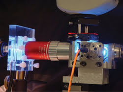
Figure 1. This fiber-based confocal microscope is built on a base plate that can be moved with 50-nm precision using piezoelectric actuators. An electric field is applied to the sample through liquid electrodes.
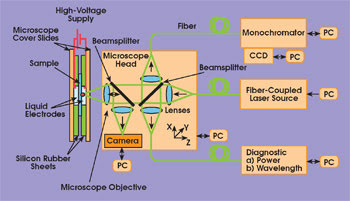
The experimental setup includes a fiber-based confocal luminescence microscope in which the fiber ends function as pinholes (Figures 1 and 3). The fiber-coupled 488-nm light is focused onto the sample via a microscope objective with a 0.7 NA and a 6-mm working distance.
The sample sits in a holder that allows the application of a bias electric field that is about 30 percent lower than the coercive field required for domain inversion. However, nucleation of small inverted domains occurs in the vicinity of the laser focus. Their growth can be guided by moving the laser along the sample. Thus, direct writing of domain patterns is possible. The group demonstrated small features on the order of 1 μm, with feature size limited by the laser spot size.
Although the details of the process are still under investigation, it is clear that photoionization of trace impurities (such as Fe2+/Fe3+ ) plays a crucial role. Within the laser spot, the sample will be positively charged, leading to space-charge fields that add to the already applied field. Combined, the fields are high enough to trigger domain inversion.

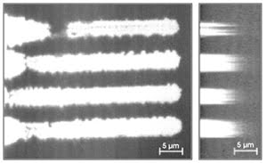
Figure 2. Vertical and horizontal cross sections of a domain pattern directly written in LiNbO3 were imaged using the change of average emission wavelength in the green spectral regions of intentionally doped erbium ions. Writing parameters were chosen to obtain a 15-μm period with small domain depth. The technique can produce a complete 3-D image.
In discovering and studying the process, the researchers made use of the capability to image the inverted domains instantly by detecting changes in the emission spectra from rare-earth ions, traces of which have been doped intentionally (Figure 2).2,3 Although intentional doping offers the highest sensitivity, scientists also can exploit luminescence from trace defects and Raman spectra for imaging purposes.
The microscope setup can detect and evaluate spectra at speeds as fast as 100 Hz, providing instantaneous feedback for precision control of nucleation and growth of domains. This way, parameters for the production of particular patterns can be optimized in situ and then easily adapted for variation in the crystal composition.

Figure 3. The microscopy technique illustrated in this schematic focuses 488-nm light onto a sample through an objective with a 6-mm working distance.
So far, the Lehigh team has demonstrated only two-dimensional patterns. Ongoing research will exploit the resolution of a confocal microscope to obtain control of domain growth in three dimensions.
References
1. V. Dierolf and C. Sandmann (May 17, 2004). Direct-write method for domain inversion patterns in LiNbO3. APPL. PHYS. Lett., pp. 3987-3989.
2. V. Dierolf and C. Sandmann (February 2004). Inspection of periodically poled waveguide devices by confocal luminescence microscopy. APPL. PHYS. B, pp. 363-366.
3. V. Dierolf et al (Feb. 15, 2003). Ferroelectric domain imaging by defect-luminescence microscopy. J. APPL. PHYS., pp. 2295-2297.
Meet the authors
Christian Sandmann and Volkmar Dierolf are with the physics department and Lehigh Center for Optical Technologies at Lehigh University in Bethlehem, Pa.; e-mail: [email protected].