ANTONIO CASTELO, EUROPEAN PHOTONICS INDUSTRY CONSORTIUM (EPIC)
Laser microprocessing covers a broad scope of laser processes used in the machining of ultrafine structures. In this area of technology, micrometer-scale levels of precision and accuracy are required to obtain the desired structures and, more critically, ensure the functionality of produced parts. The rise in the number of markets and applications for these processes in recent years corresponds to the increasingly demanding requirements from end users, in terms of throughput as well as precision.
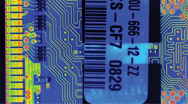
As advancements in laser microprocessing flourish in the semiconductor sector, process monitoring, including via SWIR imaging, is further increasing the chances to achieve favorable outcomes in processing compact components. Courtesy of New Imaging Technologies (NIT).
To meet necessary thresholds, industry players are spearheading developments
to laser sources and the additional
components that complete the modern workstation. Ultrashort-pulse lasers, high-performance operability at MIR wavelengths, scanners, robots and movement stages, software, and integration capabilities are among the active areas of innovation.
At the same time, process monitoring is reaching new levels of functionality, providing a means to control the laser process in-line and ensure the quality of the produced parts.
The semiconductor and consumer electronics industries are two prominent adopters of these advancing technologies. For example, both sectors benefit from the advantages that industrial lasers provide for the various processes needed for the manufacture and refinement of wafers, displays, and circuit boards.
As virtually every feature of the components found and used in these industries has become smaller, current versions require higher precision from processing steps as well as finished parts. The architectures of electronic components pose a particular challenge; these parts consist of multiple layers that could each comprise very different materials. Further, cleanness must be ensured in the manufacturing process. The combination of these factors compounds the challenges of the laser systems tasked with enabling such precision processing.
Source optimizations
Femtosecond lasers are already an advanced optical processing technology, and generally address extremely demanding requirements. Still, improvements to durability and performance are further driving these lasers into challenging processing environments.
Lithuania-based Litilit has developed a range of industrial femtosecond lasers for these processing functions, including a class of industrial lasers that achieves a burst mode with a virtually unlimited pulse number in the package, and up to 400-µJ pulse energy per burst. These lasers offer emission wavelengths of 1030 nm and 515 nm, pulse widths between 400 fs and 4 ps, and repetition rates
between 100 kHz and 1 MHz.
Given the wide range of applications
— which corresponds to a range of performance requirements — that command these high-performance industrial femtosecond lasers, Litilit is engaged in application trials, and in one case the company explored the laser etching of copper electrodes on glass substrates. In these trials, Litilit removed the copper layer from different glass substrates and created a structure with minimal damage to the substrate. Further observations revealed no delamination or defects of the copper layer after the laser process.
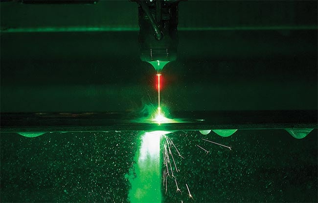
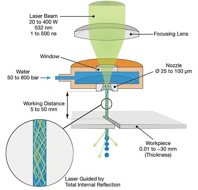
An image (top) and the scheme (bottom) of Synova’s laser MicroJet (LMJ) technology. The solution combines a laser with a water jet that precisely guides the beam via total internal reflection. The technology can thereby resolve problems, such as thermal damage and debris deposition, that commonly plague nanosecond lasers in industrial use cases. Courtesy of Synova.
Certain hybrid machining methods enable the use of nanosecond lasers for high-throughput processing tasks for the semiconductor and consumer electronics industries, while mitigating the drawbacks that are inherent to these sources. One example is Synova’s laser MicroJet (LMJ) technology, which combines a laser with a thin water jet. This jet uses total internal reflection to precisely guide the beam in a manner similar to that which can be achieved via conventional optical fibers. The LMJ mechanism guides the laser beam over distances of up to 10 cm without requiring focusing or distance control, enabling narrow and highly parallel cuts in materials from 1 to 40 mm in thickness, as shown in the figure on this page (page 63).
Synova’s LMJ technology resolves
significant problems that are commonly associated with nanosecond lasers: thermal damage, contamination, deformation, debris deposition, oxidation, micro-cracks, and taper. The technology can also be used with UV, visible, and NIR sources.
Applied to the semiconductor and consumer electronics industries, the LMJ method enables the cutting, grooving, and dicing of sensitive materials, resulting in smooth edges, high wafer fracture strength, and an overall reduction in the risk of breakage. Further, this technology enables precise cutting of various semiconductor materials, such as silicon, gallium arsenide, silicon carbide, low-K dielectrics, and even coated materials such as epoxy-molded compound wafers of various thicknesses between 50 µm and 2 mm.
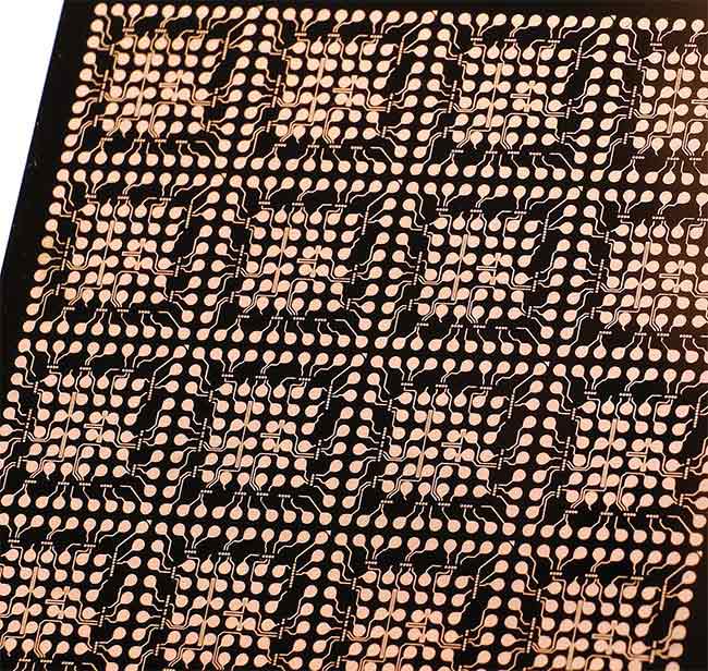
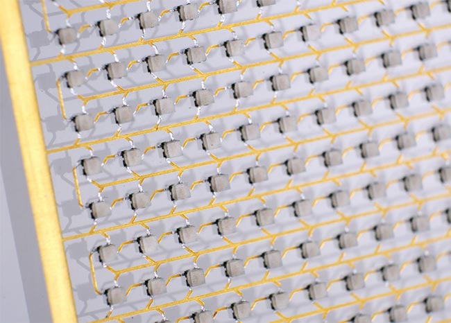
Conductive traces formed on a dielectric material via Selective Surface Activation Induced by a Laser (SSAIL) method technology.
Courtesy of Akoneer.
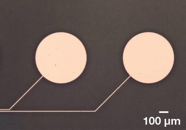
In trials demonstrating the laser etching of copper electrodes on glass substrates, femtosecond laser developer Litilit removed the copper layer from different glass substrates, including Corning Eagle XG and fused silica glass. Courtesy of Litilit and Workshop of Photonics.
For semiconductor fabrication specifically, Synova’s technology also enables multidirectional 2D cutting, high throughput processing of thick semiconductor equipment. Applications include silicon showerheads and silicon carbide susceptor plates, as well as the downsizing and detouring of wafer ring holders.
Meeting material demands
Transparent conducting films (TCFs) present another compelling use case for advanced laser processes. These thin films can carry electricity when deposited on substrates of glass, silicon, and/or polymers, which makes them important components in devices such as OLEDs, touch screens, and LCDs. Both indium tin oxide and doped zinc oxides are largely used, due to their excellent transparency
and electrical properties. Newer materials, such as graphene oxide and PEDOT, also show promise for flexible electronics due to their excellent bending behaviors.
Industry has used several laser processes since the 1990s to perform various tasks on TCFs. These include pulsed laser deposition to grow transparent conducting oxides on different substrates; laser annealing to enhance the crystallinity of the films; and etching to obtain grooves on transparent electrodes. Lasers have also been used for patterning, which can be used to remove some parts of the material layer to functionalize the surface’s electrical properties and generate a circuit.
In patterning TCFs, two primary challenges place heightened demand on the laser system. First, it is required to selectively remove the thin film without affecting the substrate. The laser must also be used to perform back processing — removing the layer through the substrate — since this procedure may be preferable for certain applications.
To address these challenges, Québec City-based Femtum, a portfolio company of Germany’s ELAS Technologies Investment, has developed a MIR-pulsed fiber laser at 2.8 µm for selective removal of TCFs on different substrates. MIR-pulsed lasers are advantageous for thin-film patterning because they are based on oxide materials that strongly absorb at wavelengths ~3 µm. Compared to UV or NIR-laser patterning, it is easier to selectively remove these thin layers without affecting the substrate, since the substrate possesses a much higher ablation threshold at these MIR wavelengths. Femtum’s solution enables users to precisely process TCFs on various substrates, including flexible polymers or other MIR transparent substrates, such as silicon and germanium, to thereby achieve very small feature sizes.
Fabricators are also applying novel laser methods to processing tasks in the consumer electronics and semiconductor industries. The Selective Surface Activation Induced by a Laser (SSAIL) method, developed by the Center for Physical Sciences and Technology (FTMC) in Lithuania, is one such method. This technique derives from the objective to solve emerging production issues for electrical conductors on polymers, such as the formation of electrical circuit traces on 3D-shaped dielectrics. SSAIL comprises three steps: laser modification of the dielectric surface, which is achieved by scanning the surface with the beam; chemical activation of the modified areas; and electroless plating of the activated parts.
Lithuanian company Akoneer has implemented this technology in its laser micromachining workstations, which
are used for applications such as high-resolution conductive traces on polymers, glasses, ceramics, silicon, and other
dielectric materials. It enables tighter electronics packaging on flat or 3D surfaces, with traces down to a width of
1 µm in some materials, making antennas directly on/in parts and creating functional surfaces.
Monitoring process
Visual inspections have traditionally been used for quality control in the production processes of consumer electronics. However, as components have become increasingly sophisticated, some inspection tasks today — for example, the evaluation of weld seams — can only be assessed with an automated monitoring system. These in-line and on-line inspections are critical, especially when applied to an industry that demands high production rates.
Automated laser and 3D measurement technology company Precitec is precisely addressing this dynamic. Its Laser Welding Monitor (LWM) 4.0 real-time quality monitoring system records the emission signals of the welding process as it happens. Recorded data is compared with reference curves to report any deviations to the higher-level control system, also in real time. As a result, error detection takes place at an early stage to ensure the stability of the monitored process in the long term. Such a system is particularly valuable for monitoring processes involving mixed joints of aluminum, stainless steel, and copper.
In the imaging domain, SWIR cameras are favored for semiconductor inspection due to the capability of SWIR light to “see” inside silicon to detect cracks and other potential wafer defects, or defects to solar cell panels. SWIR imagers are further used to perform failure analyses of integrated circuits. New Imaging
Technologies’ (NIT’s) line-scan array camera solution, for example, which is based on an indium gallium arsenide detector, provides extremely sharp images of defects in materials at a high throughput. This system achieves 2K resolution (2048 × 1 pixels at 7.5-µm pixel pitch). NIT has also recently launched a high-resolution SWIR sensor for the most demanding inspections in this field, with an 8-µm pixel pitch and 2-MP resolution
at 1920 × 1080 pixels. This solution achieves ultralow noise of 25 e- to ensure image clarity even in challenging environments.
Ensuring a prolific combination
Together, advancing laser technologies and process monitoring solutions are shifting the landscape of the consumer electronics and semiconductor industries. To drive the adoption of these laser-based advanced manufacturing technologies, consortia and networks — already established and new to form — are committing
to support the photonics companies driving these product innovations as well as the semiconductor and electronics industries.
The Pan-European network PULSATE aims to connect digital innovation hubs in Europe with expertise in laser-based manufacturing technologies. PULSATE helps companies that are interested in integrating these capabilities into their production processes, as well as those interested in exploring their capabilities to make optimal implementations. Since physical, logistical, and financial entry barriers can hinder the adoption of these dynamic technologies, PULSATE serves as a single-entry point to support users and companies. This includes connecting all constituent companies with the proper partners based on need and capability, and helping the industry develop and promote trainings, technical webinars, and networking events.