BEDA ESPINOZA, TAGUHI DALLAKYAN AND PHONG DINH, MKS INSTRUMENTS LIGHT & MOTION DIVISION
Rapid prototyping is a fabrication technique that uses additive layer-by-layer fabrication to create three-dimensional structures from devices ranging in scale from MEMS devices to 3D-printed houses. The technique has its origins in the mathematical theories of Herb Voelker1 that provide the basis for 3D computer-aided design (CAD)2. Carl Deckard applied these principles in the 1990s to develop a fabrication method that he called “selective laser sintering3,” which rapidly evolved into 3D printing, rapid prototyping and other laser microfabrication methods4.
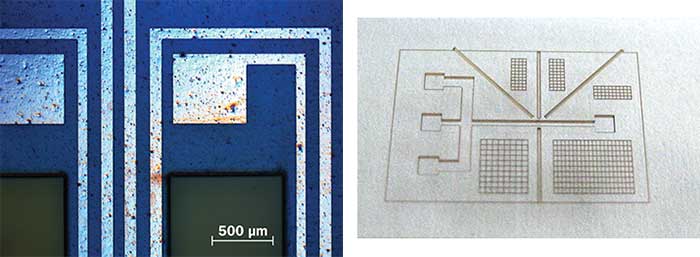
Cutting and structuring of polymers (sensors and microfluidic devices) using a high-power, ultrafast industrial laser. Courtesy of MKS Instruments Light and Motion Division.
Recently, rapid prototyping has captured the interest and imagination of the public owing to the potential for easier and cheaper access to everything from replacement parts for common consumer products to dental appliances5. President Barack Obama, in his 2013 State of the Union address, promoted rapid prototyping as having the “potential to revolutionize the way we make almost everything.” Rapid prototyping machines are now common in many settings, from private homes to the engineering departments of major corporations.
According to D.V. Mahindru and Priyanka Mahendru6, there are at least six different rapid prototyping techniques commercially available:
• stereo lithography,
• laminated object manufacturing,
• selective laser sintering,
• laser beam machining,
• solid ground curing, and
• 3D inkjet printing.
All of these techniques have certain basic steps in common. A 3D CAD model must be developed and converted to a stereo lithography format model that can be sliced into thin cross-sectional layers. The geometrical information from these layers is used to control equipment that performs the operation — laser ablation, powder fusion, polymerization, additive printing — necessary to construct the artifact on a one-layer-at-a-time basis.
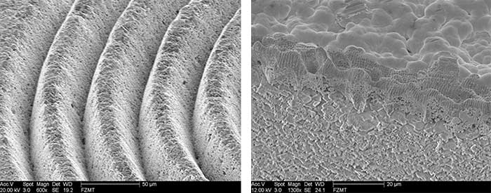
Surface structuring of AlO2 ceramics using a femtosecond laser. Right image with gold coating on the surface. Courtesy of MKS Instruments Light and Motion Division.
Rapid prototyping tools for micromachining and microfabrication benefit from high-intensity, ultrafast femtosecond lasers that produce extremely localized heating and no collateral damage or heat effects in surrounding materials — a minimal heat affected zone (HAZ). Along with an ability to focus the beam to a small (1 µm) spot size, the minimization of adjacent heat-affected zones is fundamental for the production of high-quality three-dimensional micro- and nanostructures. Optical components are needed that manage the laser beam from the source to the material being worked as is software to translate 3D CAD formats into executable machine instructions. Ancillary components including power meters, beam profilers, galvo scanners (control mirrors), etc., ensure repeatability in the optical characteristics governing the process. Motion stages offer fast, accurate and precise positioning of both the laser beam and the substrate at the nanometer scale, determining the precision with which microfeatures can be added or removed in the fabrication process and the manufacturing time requirements. Finally, controllers are required to drive the motion stages and synchronize their motion with the laser pulses and the ancillary devices.
Notably, rapid prototyping systems can be configured using “off-the-shelf” lasers, optical software and motion control tools.
Laser micromachining
Laser micromachining is a subtractive machining process in which the thermal energy of a laser is used to ablate or otherwise alter metal or nonmetal surfaces. The basic components of a laser micromachining tool include a device for scribing and ablation processes on a 6-in. silicon wafer (Figure 1). The tool contains optical and motion control subsystems that are synchronized and controlled using a computer running specialized laser micromachining software.
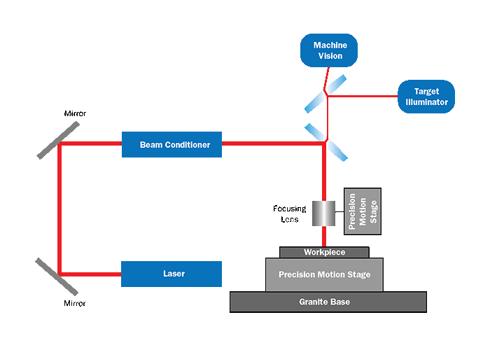
Figure 1. Components in a laser micromachining tool. Courtesy of MKS Instruments Light and Motion Division.
A wide variety of lasers are employed in advanced micromachining applications. One example is an automated, high-power (10- to 20-W) fast-pulsed laser such as the Spectra-Physics Spirit industrial femtosecond laser. Adjustable pulse energy and repetition rates (up to 40 µJ and 1 MHz, respectively) allow precise control of the energy delivered to the workpiece, minimizing the HAZ. The optics system consists of the laser, galvo scanners, a beam collimator, and a focusing lens along with the lenses and illumination needed for observing the workpiece.
The motion control system is mounted on a granite base to ensure stability and repeatability in the movement and positioning of the workpiece. The system uses synchronized precision motion stages such as Newport’s XML210 and XMS160 to position the workpiece in the XY direction and the focusing lens in the Z direction. Optionally, a stage for rotary positioning of the workpiece can be stacked on the XY stage. For micromachining applications, these stages require positioning accuracy on the order of ±0.5 µm with a repeatability of <0.05 µm in XY directions. Positioning accuracy requirements in the Z direction are somewhat more forgiving at <5 µm, with resolution specifications typically about 0.1 µm. Travel range in the XY directions for applications such as the one in this discussion (the workpiece is a 6-in. diameter silicon wafer) is minimally 160 mm (slightly greater than the workpiece diameter) with minimal incremental motion of 0.010 µm. Translational speeds on the order of 300 mm/sec and accelerations of up to 5 m/sec2 are required in each axis to ensure reasonable throughput. Motion of the workpiece and lens is controlled and synchronized using an integrated motion controller/driver to control movement in the X, Y and Z directions (and rotational motion, where equipped). The system requires specialized software for laser machining and machine vision. This software translates the 3D CAD model into adjustments to the stages, galvo scanners, optical components laser sources, sensors, power meters, etc.
Figure 2 shows a 3D drawing of a laser micromachining system, along with an image of a real-world motion control system for use in such a tool. The design employs a dual optical system to allow special beam routing for two wavelengths and beam collimation depicted in the 3D schematic (Figure 2a). These types of systems have been used to produce microstructures such as optical waveguides.
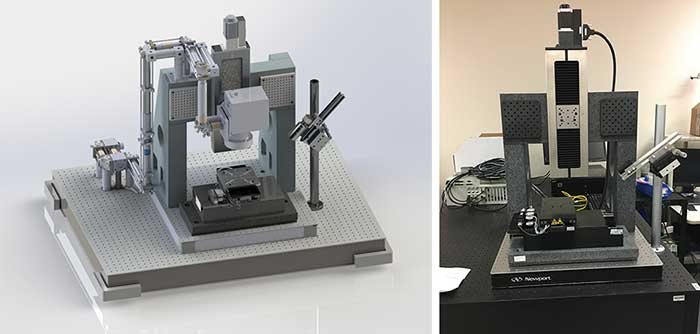
Figure 2. Laser machining assembly 3D schematic (a); motion control system (b). Courtesy of MKS Instruments Light and Motion Division.
Ablative laser micromachining is considered mature technology in a number of industries. Automotive applications include the fabrication of fuel injector nozzles, part marking and microwelding. In consumer electronics, laser micromachining is employed in applications such as glass cutting and structuring for OLEDs.
Additive micromanufacturing
Three-dimensional additive microfabrication is the opposite of laser micromachining in that it creates a microstructure using layer-by-layer material addition through sintering, or some other mechanism of solidification of a source material, rather than by removing material from an already solid substrate. In additive microfabrication, the laser beam provides the energy necessary for patterned, layer-by-layer fusion of solid materials (sintering) or for a patterned, layer-by-layer polymerization (stereolithography or two-photon polymerization)7,8. As with laser micromachining, additive microfabrication can benefit from femtosecond lasers to minimize HAZ and, in the case of two-photon polymerization, to deliver the high local photon densities necessary to induce localized polymerization.
Two-and-a-half- and three-dimensional additive micromanufacturing is finding applications in the fabrication of complex microstructures in many areas, including electronics, microfluidics, MEMS, micro-optical electro-mechanical systems (MOEMS), biomedical, chemical analysis and decorative surface structures, to name a few. It can produce these microstructures from a wide variety of materials, ranging from metals and alloys to ceramics and polymers. For many applications, additive micromanufacturing is superior to conventional photolithographic patterning for micro- and nanoscale device fabrication since it can create high-aspect-ratio structures with fully vertical walls, re-entrant angles and other free-form structural characteristics that are impossible with conventional patterning technology. Additionally, additive microfabrication offers a more direct simplified route to such structures.
Configuring an additive micromanufacturing tool uses similar components to those employed in laser micromachining. A wide range of lasers can be used, including UV pulsed nanosecond lasers and industrial femtosecond lasers such as the 1040- and 520-nm Spirit lasers. XY and Z motion stages coupled with a granite base and bridge provide the necessary level of precision and accuracy in motion control. Additive microfabrication systems can be controlled using LMS Lite software equipped with a 3D module. Ultrafast manufacturing can be achieved through the use of controllers and drivers for high-speed multi-axis trajectory pulsing.
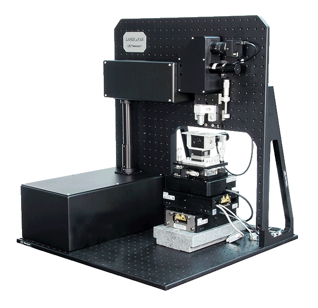
Figure 3. An integrated Laser µFab from Newport. Courtesy of MKS Instruments Light and Motion Division.
Additive microfabrication is finding practical application in areas such as MEMS for the automotive industry; microfluidics for chemical, biochemical and pharmaceutical industries; and component fabrication for optoelectronics.
A Laser µFab
The commonality of equipment requirements for ablative laser micromachining and additive microfabrication shows that the integration of these two micromanufacturing techniques into a single manufacturing tool is feasible. Newport’s Laser µFab is one tabletop tool that combines these capabilities (Figure 3). This tool, configured with a Spirit 1040-/520-nm industrial femtosecond laser, with either XMS or VP series motion stages and an XPS-Q4 four-axis controller, can process glass, metals, polymers, semiconductors or ceramics using transformative or ablative microfabrication, in addition to additive processing techniques such as two-photon polymerization and laser-assisted deposition. On-axis reflective light microscopy is used for monitoring the laser processing in real time. Customizable software controls system operation.
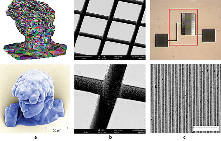
Figure 4. Microfabrication using the Laser µFab: STL file and 3D microstructure produced using TPP (10-µm scale) (a); 2D patterns on a polymer produced using laser ablation (5-µm channels) (b); laser-assisted silver deposition on glass (3.5-µm line widths) (c). Courtesy of MKS Instruments Light and Motion Division.
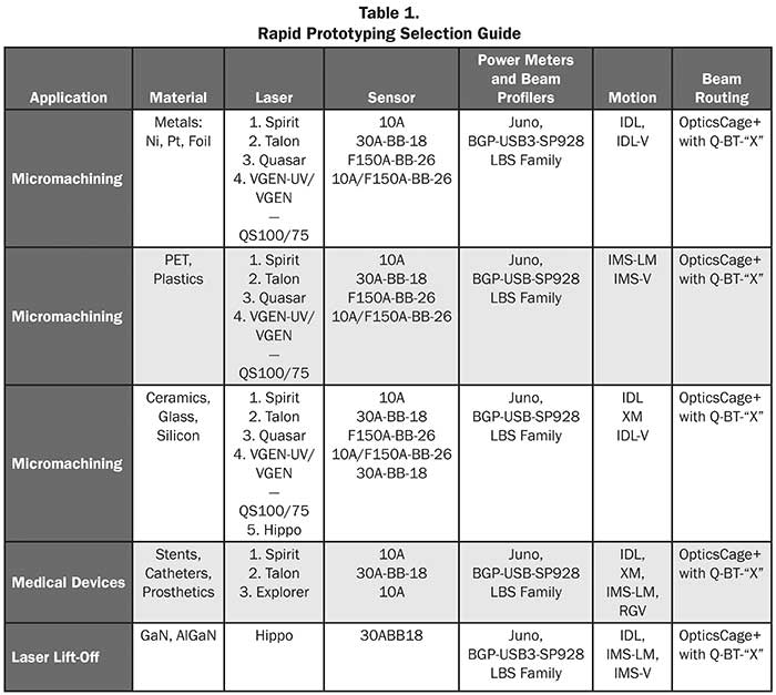
The tool can be utilized as an additive microfabrication tool (TPP), a laser micromachining tool and a tool for laser-assisted deposition to fabricate microstructures (Figure 4). Different laser microfabrication applications are appropriate for certain components (Table 1).
Laser microfabrication has evolved rapidly since the 1990s, to the point where many methods have become accepted as mature process technologies in a variety of industries. These methodologies continue to find new applications in replacing more complex fabrication protocols or in entirely new technologies.
Meet the authors
Phong Dinh is an applications engineer, Taguhi Dallakyan is a product specialist and Beda Espinoza is a product marketing manager for the MKS Light and Motion Division, located in Irvine, Calif.
References
1. H. Voelcker et al. (August 1978). The PADL 1.0/2 system for defining and displaying solid objects. Comput Graph (ACM), pp. 257-263.
2. C.M. Eastman and K. Preiss (1984). A review of solid shape modelling based on integrity verification. Comput Aided Des, Vol. 16, Issue 2, pp. 66-80.
3. J.J. Beaman and C.R. Deckard (July 3, 1990). Selective laser sintering with assisted powder handling. USA Patent US4938816 A.
4. X. Yan and P. Gu (1996). A review of rapid prototyping technologies and systems. Comput Aided Des, Vol. 28, Issue 4, pp. 307-318.
5. H. Lipson and M. Kerman (2013). Fabricated: The New World of 3D Printing. Indianapolis: John Wiley & Son.
6. D.V. Mahindru and P. Mahendru (2013). Review of rapid prototyping technology for the future. GJCST, Graphics and Vision, Vol. 13, Issue 4.
7. Application Note: Three-dimensional microfabrication by two-photon polymerization [online]. Available: https://www.newport.com/medias/sys_master/images/images/h26/hf7/8797287743518/Three-Dimensional-Microfabrication-App-Note-37.pdf.
8. Application Note: Workstation for laser direct-write processing [online]. Available: https://www.newport.com/medias/sys_master/images/images/h15/h4a/8797304651806/Workstation-for-Laser-Direct-Write-Processing-App-Note-39.pdf.