Researchers at Penn State developed a metalens that is large enough to be put into a telescope, and then they used the optic to image the moon's surface. The metalens, which the researchers used to create a metalens telecscope instrument, works in the near-infrared range with nearly diffraction-limited focal spot sizes and a high peak focusing efficiency of 80.84% at 1450 nm experimentally.
Despite the promise of metalenses, the researchers said, the aperture sizes of the devices, as engineered via traditional fabrication methods, limit their use on practical optical devices such as telescopes. The Penn State metalens measures 8 cm across, larger than most previously developed functional metalenses, which are measured in millimeters.

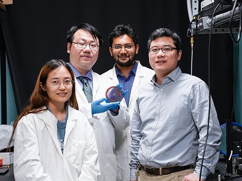
From left: Penn State electrical engineering graduate students Lidan Zhang, Shengyuan Chang, and Md Tarek Rahman, and Penn State associate professor Xingjie Ni display their flat, compact metalens, which when integrated into a telescope can image the lunar surface. Courtesy of Jeff Xu/Penn State.
Metalenses are typically made using electron beam lithography, in which a focused beam of electrons is scanned onto a piece of glass or other transparent substrate to create antenna-like patterns point by point. However, the scanning process of the electron beam limits the size of the lens that can be created, as scanning each point is time-consuming and has low throughput.
To create a bigger lens, the team used deep ultraviolet (DUV) lithography.
According to corresponding author Xingjie Ni, associate professor of electrical engineering and computer science at Penn State, this high-throughput, high-yield process can be used to produce
many computer chips within seconds.
“We found this to be a good fabrication method for metalenses because it allows for much larger pattern sizes while still maintaining small details, which allows the lens to work effectively,” Ni said.
The researchers modified the method with their own novel procedure, called rotating wafer and stitching. They divided the wafer, upon which the metalens was fabricated, into four quadrants, which were further divided into 22- × 22-mm regions — smaller than a standard postage stamp. Using a DUV lithography machine, they projected a pattern onto one quadrant through projection lenses, which they then rotated by 90° and projected again. They repeated the rotation until all four quadrants were patterned.

“The process is cost-effective because the masks containing the pattern data for each quadrant can be reused due to the rotation symmetry of the metalens,” Ni said. “This reduces the manufacturing and environmental costs of the method.”

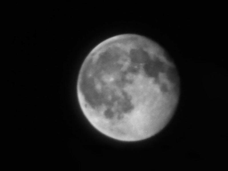
Electrical engineering researchers captured images of the lunar surface using their large-aperture metalens telescope. Courtesy of Xingjie Ni.
As the size of the metalens increased, the digital files required to process the patterns became significantly larger, which would take a long time for the DUV lithography machine to process. To overcome this issue, the researchers compressed the files using data approximations and by referencing nonunique data.
“We utilized every possible method to reduce the file size,” Ni said. “We identified identical data points and referenced existing ones, gradually reducing the data until we had a usable file to send to the machine for creating the metalens.”
Using the new fabrication method, the researchers developed a single-lens telescope and captured clear images of the lunar surface — achieving greater resolution of objects and much farther imaging distance than previous metalenses.
Before the technology can be applied to modern cameras, researchers must address the issue of chromatic aberration, the Penn State team members said. The researchers are exploring designs in the visible range, Ni said, and will compensate for various optical aberrations, including chromatic aberration.
The research was published in Nano Letters (www.doi.org/10.1021/acs.nanolett.2c03561).