Advances in on-chip integration, materials and fabrication methods enable smaller, faster components for next-generation applications.
The market for optoelectronic (OE) components – parts that make up other parts and connect between subsystems and systems – is dominated by light-emitting diodes (LEDs), which hold 79 percent of the market. Most of those LEDs are in lighting and backlights, according to the Optoelectronic Components – World – 2013 report by IHS Technologies of Englewood, Colo. The rest of this market consists of optocouplers, photodiodes and transistors, light emitters, detectors and sensors, optical switches and so on. Many of these components have a recognizable “window” or lens that passes light.
Although LEDs are quite dominant in the market, the IHS report predicts that optocouplers – especially in gate-driver applications such as hybrid and electric vehicles, photovoltaic inverters and smart meters – will grow from $543 million in 2013 to $677 million in 2018, which represents 25 percent growth in five years. The consumer electronics industry, another large user of components including ambient light sensors in smartphones and tablets, will drive 50 percent growth from $252 million in 2013 to $379 million in 2018.

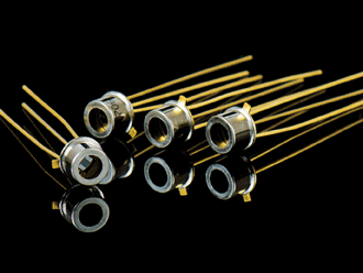
Components are sometimes characterized by a visible ‘window’ that passes light,
such as these pulsable IR emitters offered by Laser Components. Photo courtesy of Laser Components.
A key trend in OE components is the push to facilitate integration of light-based components into single, multifunctional, smaller, practical building blocks. Consumers are driving the demand for integration in the OE market because, for one thing, our most popular electronic devices – mobile phones, monitors, tablets and laptops – must provide more function in the same footprint and convert electrons to photons at ever-smaller nanoscale dimensions without increasing cost. The need for smaller, lower-cost integrated components also is driven by service providers who must meet the need for increased system capacity and higher data rates in the same real-estate footprint.
MEMS technology
Microelectromechanical systems (MEMS) technology is one way that integration of photonic and electronic components into nanoscale devices is progressing. Researchers Cai Hong and Liu Ai Qun at A*STAR’s Institute of Microelectronics and Nanyang Technological University in Singapore and a joint team recently demonstrated a prototype tiny on-chip integrated laser that is tunable from 1531.2 to 1579.5 nm; they announced the development at the 2013 International Electron Devices Meeting (IEDM) in Washington.

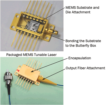
A prototype integrated MEMS laser on a chip measuring 1 × 1 cm is tunable across a 48-nm range in the near-IR. Integration of components onto chips makes them more amenable to mass production and eases their use in telecom, biomedical and spectroscopy applications. Photo courtesy of A*STAR Institute of Microelectronics/Nanyang Technological University.
The team fabricated the tuning structures using deep reactive-ion etching on a 100-µm-thick silicon-on-insulator wafer and a low-cost passive alignment approach. Measuring 1 × 1 cm, the prototype tunable IR laser – comprising a gain chip, fiber rod lens, parabolic mirror, pivoted Littrow grating and fiber-lens assembly – is the smallest reported tunable laser fabricated using MEMS technology. The on-chip laser is, at that size, 10 times smaller than most tunable lasers available on the market, and offers coupling efficiency as high as 76.5 percent compared with MEMS tunable lasers with external cavities, which max out at 50 percent efficiency.
In a demonstration, the laser achieved a side-mode suppression ratio of 28 dB. The advantages of such a small tunable laser with high coupling efficiency, along with tuning speed and ease of fabrication, make it ideal for application in wavelength-division-multiplexing networks and biomedical devices.
A wide tuning range of 48 nm usually comes at the expense of a large external cavity, Hong said.
“Our laser exploits the superior light converging ability of the rod lens and parabolic mirror of the 3-D microcoupling system to achieve both wide wavelength tuning range and small form factor,” he added. The team expects the breakthrough to help product developers design smaller, faster and low-cost devices for next-generation fiber optic networks and other tunable laser applications.
New materials foster integration
Successful fabrication of novel semiconductor materials is a hot research goal. Many new materials are making progress that can help integrate photonic and electronic components into nanoscale devices, thanks to work by researchers such as Dr. Xiaodong Xu, assistant professor of materials science, engineering and physics at the University of Washington in Seattle. In an online Nature Nanotechnology paper (doi: 10.1038/nnano.2014.26), Xu and colleagues reported that they had created the thinnest-known LEDs using flat sheets of tungsten diselenide (WSe2), a semiconductor material in a class of monolayer transition-metal dichalcogenides (TMDs) that have recently surfaced as promising candidates for emerging optoelectronic applications as a result of their interesting optical properties.
Whereas previous work found that monolayer molybdenum disulfide (MoS2), another TMD material, exhibited electroluminescence, Xu’s group found that lateral p-n junctions in monolayer WSe2 exhibit bright electroluminescence with a 1000 times smaller injection current and a 10 times narrower linewidth than that of MoS2. The LEDs are created using adhesive tape to extract a single layer of material from thicker layers. The 2-D LEDs made by Xu’s team are only 3 atoms thick, but are mechanically strong enough to be flexible, even foldable, which could make them useful in on-chip lasers and 2-D electro-optic modulators for future portable and integrated devices.

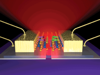
A lateral, 2-D LED made of a flat sheet of tungsten diselenide is 10 to 20 times thinner than the LEDs commonly used in today’s consumer electronics. Photo courtesy of Jason S. Ross/University of Washington.
The study also showed that because of the potential valley polarization of the excitons in these new materials, electroluminescence generated in the LED could eventually be made to be either right or left circularly polarized. This could lead to completely new LEDs that would enable controllable encoding via polarization – i.e., a new type of bit. New types of spin- and valley-polarized LEDs could enable new computational schemes in photonic circuits, said first author Jason Ross, who is a graduate student in Xu’s laboratory.
In the same issue of Nature Nanotechnology, groups from MIT and Vienna University of Technology in Austria also published complementary results of their research on WSe2, further describing the electrical properties of such an LED device and the performance of the device as a solar cell.
“The main challenge before us is the mass production of two-dimensional materials; specifically, the ability to grow large, wafer-sized pieces,” Ross said. “These recent papers involve single pieces of the WSe2 material that are, in lateral dimensions, about the thickness of a human hair (80,000 to 100,000 nm wide). Many groups worldwide are investigating chemical and physical vapor deposition schemes to grow a large single crystal, but have so far been unsuccessful.”

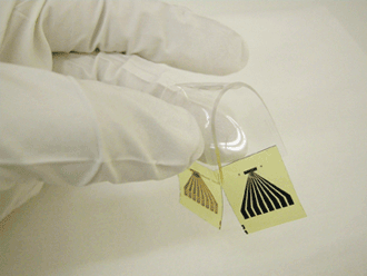
The first truly stretchable optical interconnect made of rubbery PDMS material integrates a VCSEL array, a four-channel waveguide and an embedded photodiode detector for use in robotic limbs or wearable sensors. Photo courtesy of
Centre for Microsystems Technology/imec/Ghent University.
In another direction, researchers at the Centre for Microsystems Technology (CMST), imec’s associated lab at Ghent University in Belgium, have created a miniature optical circuit that uses integrated optoelectronic components to read out a miniature optical waveguide array made of a bendable, stretchable rubbery material. In work reported in Optics Express in February (doi: 10.1364/OE.22.004168), lead author Dr. Jeroen Missinne and colleagues reported using a transparent, stretchy, commercially available material called polydimethylsiloxane (PDMS) to create the first truly stretchable optical link with integrated light sources and detectors.
The device guides light along its path from an integrated 1 × 4 vertical-cavity surface-emitting laser (VCSEL) array emitting at 850 nm on one end through four PDMS waveguides to a photodiode detector array coupled to the other end, even when the material is stretched up to 30 percent of its length and bent around an object as small as a finger. The new connector consists of a transparent core of PDMS that transmits the light, with a surrounding layer of PDMS of a lower refractive index that traps the light in the core material. The guide remained reliable through a test in which the team stretched it to 10 percent elongation of its original length 80,000 times.
Although traditional fiber can send light around gentle bends, the group says the device may be the first to couple light in and out of miniature optical waveguides, even when they are bent or stretched. The new optical link is cost-efficient to fabricate and could be used in networks of wearable body sensors, robotic limbs or bendable consumer electronics, Missinne said. The next step for the researchers is to reduce the diameter of the waveguide from 50 µm down to just a few microns.
Merging such components into practical devices may happen soon in all kinds of emerging applications.