Solid-state photomultipliers compare well with traditional devices
Wayne Seemungal, Amplification Technologies Inc.
Vacuum tube technology has always preceded its solid-state counterpart. The most familiar example of the former is the transistor, considered the greatest invention of the 20th century. Other examples are cathode-ray and electronic amplifier tubes. Advances in materials technology have allowed all of these to be replaced by solid-state alternatives.
The photomultiplier tube (PMT) is one of the last types of vacuum tube technologies still in use. Traditional vacuum tube photomultipliers are hard to match for sheer noiseless amplification of photoelectrons (160 dB). In some ways, they have superior features when compared with other detectors: High frequency response, low timing jitter and a single detector can cover up to 10 in. in diameter.
A new solid-state technology, dubbed silicon photomultipliers – although the technology can be implemented in many other materials systems – has finally arrived, matching the performance of photomultiplier tubes and even surpassing it in some cases.
The choice of silicon versus traditional PMT can be a function of the specific application requirements. This article will explore uses for various types of photon detection technologies and share developments in solid-state. It also will give the reader an understanding of which technology is most appropriate based on application needs.
According to Wikipedia, the first patent for a vacuum-based amplifier was filed in Canada by Julius Lilienfeld in 1925. This was for a field-effect transistor. Twenty years later, in search of higher frequency amplifiers needed for radar, workers at Bell Labs developed the first semiconductor transistors. The first vacuum tube photomultipliers date to early 1934, capitalizing on the photoelectric effect for which Albert Einstein received the 1921 Nobel Prize in physics. Within two years, the device was perfected; it has changed little since. It is only recently that a solid-state replacement has become possible.
Vacuum tube technology has certain obvious shortcomings. For one, dynode multiplication necessitates a large package. Operation at high voltage requires large power consumption. Monolithic arrays are very difficult, with low yields on photocathode quantum efficiency and uniformity, and are limited in size. Then there is the issue of maintaining a vacuum.
In today’s world, the buzzwords are “leaner, greener, faster and smarter,” or LGFS. These can be applied to all technologies, not just automobiles. For photodetectors, only semiconductors hold such promise. The semiconductor photomultiplier was invented by scientists at Amplification Technologies Inc. about 10 years ago. The original design has spawned an entire new class of photodetector devices based on controlled Geiger-mode avalanche operation.
Breaking new ground
Avalanche photodiodes (APDs) with limited gain have been a standard technology for many years, but achieving controlled, high-gain electron amplification by operating in the Geiger regime was a significant challenge that has now been solved. These devices hold the promise of replacing vacuum tube PMTs and even doped-glass electron multipliers, such as microchannel plates, in many applications. They fit the LGFS profile: They consume far less power, operating at one-tenth the voltage of PMTs; there are no compounds used in fabrication that pose a danger to the environment upon disposal; and they are adaptable to a variety of applications, as any size array format is possible on a semiconductor wafer.
The latter extends the range of capabilities of these devices beyond replacement for single-channel PMTs. Consider extending the detection capability of CCD cameras down to the single-photon level, without deep cooling of back-thinned arrays (room temperature operation). Or consider high-resolution night vision arrays with high sensitivity, without the downside of image intensifiers.

Traditional silicon photomultiplier technology is based on arrays of Geiger-mode APDs. Several manufacturers have products based on this technology, but the technology still is not considered mature; i.e., several device designs exist.
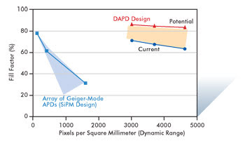
The traditional structure has a limitation in having a trade-off with photon detection efficiency. Also, the basic design is not flexible, not allowing customization for specific applications. The current design from Amplification Technologies – dubbed DAPD, or discrete amplification photon detector – consists of specially designed discrete amplification elements. These include a multichannel threshold avalanche amplifier and a reader for the amplified charge packets.

Figure 1. The design of a discrete amplification photon detector permits trade-offs among various parameters to optimize it for specific applications.
The design allows trade-off among various parameters to optimize a device for a specific application (Figure 1). The detectors perform analog detection of short pulses – down to single-photon levels – over a wide spectral range. Recently, the technology has been implemented in InGaAs, extending the spectral sensitivity to the near-infrared. The electron multiplication process is a binary amplification in separate channels that is nearly noiseless. The measured excess noise factor for these devices is typically less than 1.05 at room temperature, better than the best cryogenically cooled single-photon detector.
Important advantages of discrete-amplification technology are its wide operating voltage range, and its voltage and thermal stability. The discrete-amplification device can be operated up to 10 V above the breakdown voltage. The measured results show that the operating voltage variation is less than 30 mV/°C, and the gain variation, less than 0.5%/°C. These performance benefits enable the development of large detector arrays that would use a single reverse bias, with array elements having only minor variations of basic parameters at the same voltage.
Another advantage of semiconductor devices is their insensitivity to magnetic fields, which is a major problem for photomultiplier tubes. This is very important in large physics experiments and for future medical applications that hope to fuse images from PET and MRI or CT and MRI.
The age of silicon
So it appears that the time has come where a solid-state technology to replace vacuum tube photomultipliers is a reality. This is not to say that light-detecting photomultipliers will disappear. On the contrary, the technologies will coexist because there are applications where it may be impossible or impractical to use anything but a photomultiplier tube; for example, neutrino detectors must cover large real estate to capture just one of these elusive particles. Only thousands of photomultipliers with 10-in. photocathodes are a practical choice.
Some large physics experiments, however, would be better served by silicon photomultipliers, and beta testing has already begun. The flexibility of the semiconductor technology, however, gives it a much broader application because it can be used not only for light detection across the entire electromagnetic spectrum but also for ion and charged-molecule detection, such as in mass spectroscopy. Undoubtedly, people will find unique applications for this technology that may not be obvious at the present time.

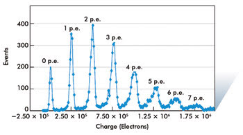
Figure 2. Discrete-amplification technology provides fast response times as well as high gain-bandwidth. p.e. = photoelectrons.
Fast response time of a photodetector is important for many applications, especially those involving measurements within a narrow time gate. Discrete-amplification technology provides very fast response as well as a high gain-bandwidth product, a prerequisite for the high-speed detection of low-level signals. The response time of a single-electron-response pulse as an output of a 1-mm active-area-diameter DAPD is approximately 1.4 ns full width half-maximum (FWHM) at the gain level of 2.8 × 10⁵. The timing resolution of the detected pulses, evaluated as the transit time spread (jitter) distribution at FWHM, is less than 300 ps (Figure 2).
Meet the author
Wayne Seemungal is business development manager of Amplification Technologies Inc. in Brooklyn, N.Y.; e-mail: [email protected].