Laser World of Photonics, June 26-29, 2017, Munich Trade Fair Center, Munich
Laser World of Photonics provides a spotlight for promising newcomers, industry veterans and innovative companies. And with tens of thousands of people from countries around the globe attending the show, that spotlight is huge.
In 2015, the biennial event — sponsored by Messe München International — featured a record number of trade fair exhibitors and hosted more than 30,000 attendees representing nearly 80 countries.
“Laser World of Photonics has an international focus. [It] covers the entire market of optical technologies — from components to systems — and addresses a huge number of industries,” Katja Stolle, executive director of Laser World of Photonics, told Photonics Media. “By attending the show, visitors gain an overview on the developments of the whole industry.”
A focus this year will be on the intertwining of medical advancement with photonics techniques and technologies. Light-based technology works well in the imaging and study of living cells, neural brain processes or medically altered tissue.

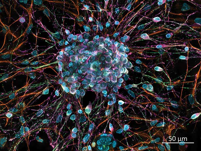
Primary neural cells in culture. The biomedical and life sciences sectors will be a focus at Laser World of Photonics 2017. Courtesy of H. Braun/LSM Bioanalytik GmbH.
“Research is proceeding at breakneck speed,” said Messe München. “Brain functions and cognitive processes are proving increasingly amenable to being controlled to permit their systematic investigation. Even the activities of individual neurons can be observed. Femtosecond lasers are being employed because they enable light manipulation even in deep brain areas. At the same time, they deliver 3D live transmissions from the functioning brain by means of multiple photon stimulation.”
Also scheduled for discussion at Laser Munich are optical techniques (notably laser technology and imaging) that assist in diagnosing diseases, surgical treatment determinations and medication developments. Optical techniques are being used in the development of miniaturized biochips and fabrication of customized 3D-scanned and 3D-printed implants, as well. Practice-oriented educational application panels will examine these and other optical technologies, research and trends. Among these tracks are:
• Photonics-Based Methods in Microscopy and Modern Operation Theaters
• Laser Applications and Optical Diagnostics in Ophthalmology
• Visions for Future Diagnostics (Imaging)
• Laser Evolution Drives Innovation in Life Sciences and Bioinstrumentation
Another focus at Laser Munich is in the industrial sector, particularly laser technology and sensor advancements that currently drive manufacturing and production.

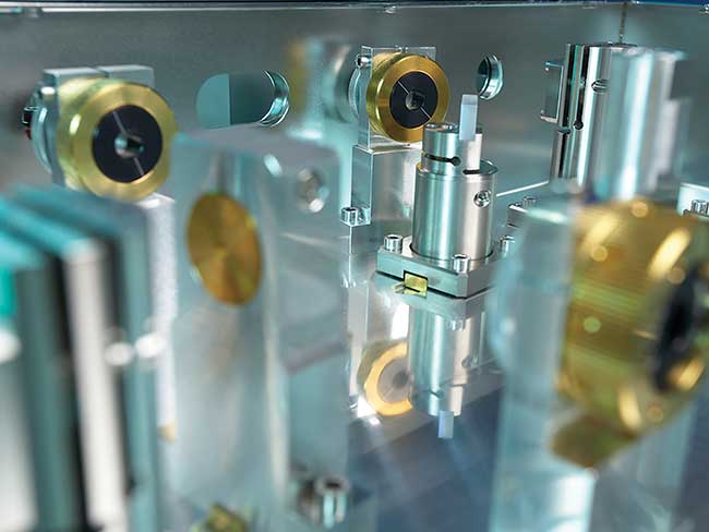
The inside of an ultrashort pulse laser. Such systems will be featured during Laser World of Photonics 2017. Courtesy of Trumpf.
“Precisely applied and digitally controlled laser technology is now absolutely essential,” said Messe München. There exists great potential for digital production, specifically in cold material processing using ultrashort laser pulses. Traditional lasers can physically impact materials (metals, plastics, glass, etc.), while newer devices that use concentrated light work without contact, eliminating the risk of corrosion.
Application panels covering the industrial sector will focus on such technology. These sessions include:
• Simulation in Photonics
• Industrial Success Stories for Applications of Ultrashort Pulsed Laser Systems
• Lasers in Microelectronics: The Smart Connected World Approaching
• 3D Printing: Laser-based Additive Manufacturing for Metal Parts
• Smart Laser Solution for Smart Mobility
• Laser Processing of Dielectric and Brittle Materials
Photonics Congress
The World of Photonics Congress, colocated with Laser Munich, offers the latest developments in research, technology and emerging applications. This year, digital optical technology is an overarching conference theme, with design, fabrication and functionality in focus.

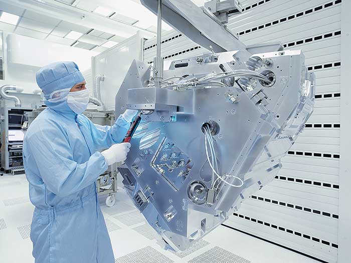
High-precision lithographic optics, such as this one by Zeiss, potentially could expose wafers using extreme UV light. Laser World of Photonics 2017 will shine a spotlight on novel technologies. Courtesy of Zeiss.
Discussions will emphasize numerical algorithms to help devise novel optics from macroscopic (used in freeform optics) to nanoscopic (used with metamaterials and plasmonics) scales. Also to be discussed is novel digital lithography and freeform mold diamond-turning techniques, as well as computational techniques to enhance functionality in imaging and display, and digital switching, tuning and reconfiguration of optics functionality.
Among other sessions slated for the 2017 Congress are Lasers in Manufacturing, EOS Optical Technologies and Optical Metrology.
The European Conference on Biomedical Optics (ECBO) is part of the Congress, as well, and will be held this year in conjunction with the ninth scientific meeting of the Head and Neck Optical Diagnostics and Intervention Society (HNODIS). Technologies such as elastic scattering spectroscopy (ESS), differential path-length spectroscopy (DPS), NIR spectroscopy, Raman spectroscopy, confocal reflectance microscopy (CRM), fluorescence imaging, microendoscopy, optical coherence tomography (OCT), lasers, photodynamic therapy (PDT) and photochemical internalization (PCI) will be topics of discussion.
Exhibition
Rounding out Laser Munich is its exhibition. This part of the event is substantial, said Messe München. In fact, Laser Munich in 2015 saw a record number of exhibitors — more than 1200 from 42 countries.

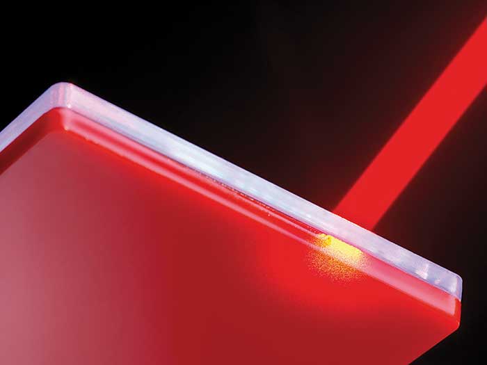
In laser plastic welding, new systems record real-time temperature curves by means of a pyrometer, which supports closed loop control. Unveiling technologies such as this makes Laser World of Photonics an innovation playground. Courtesy of Rofin.
All sectors of the industry are represented, from imaging, sensing and metrology to lasers and laser systems, biophotonics and manufacturing. Companies showcase new products and innovative technologies. Among those to be unveiled at Laser Munich are a camera developed by e2V that features a back-illuminated EMCCD sensor; Scanlab’s fiber connection technology for scan systems; and a core-centering, 3-axis splicer from Fitel.
Other exhibitors include Andor Technologies, Laser Components, KM Labs, InnoLas Photonics, Jenoptik and Piezosystem Jena. A full list of exhibitors, as well as more information about Laser World of Photonics and the World of Photonics Congress, is available at www.world-of-photonics.com.
Startup World
Startup World puts innovation at center stage during Laser World of Photonics. It offers a platform on which young companies (under five years old) can present their products and novel work in front of industry professionals.
For exhibitors, potential sponsors and financial backers, connecting with companies turns Startup World into an innovations marketplace. According to Messe München, “in many cases, the best ideas for unconventional solutions are born in discussions with these talented innovators.”
Photonics Award
As with the Startup World initiative, the Photonics Award is a place for innovation to shine. This competition recognizes the best new products in all optical technologies from startup companies. Award entries are evaluated based on business potential, level of innovation, usability, technical feasibility and product availability.
Six companies participated in 2015, with two claiming wins — Nanolive and Femtoprint. Nanolive was recognized for its 3D cell explorer, a microscope technology that enables observation of live cells in 3D without damaging them. Femtoprint presented a laser-based 3D printing solution for manufacturing nanodevices made from glass or transparent material.