Recent advancements in the high-temperature operation of terahertz (THz) quantum cascade lasers, combined with their frequency agility and the potential to operate as frequency combs and high-speed detectors, make them highly appealing for THz photonics. Building on previous approaches to THz integration, including hybrid plasmonic waveguides, monolithically integrated THz transceivers, coupled cavity devices, and, most recently, devices integrated on silicon, researchers at ETH Zurich presented a novel platform for broadband coherent THz photonics based on high-confinement active and passive planarized double metal waveguides. In the researchers’ architecture, the active and passive elements were integrated in a double-metal, high-confinement waveguide layout planarized with a low-loss polymer.
The researchers used a common metallic ground plane to demonstrate the integration of several active and passive THz photonic components onto the same platform, in an approach that allowed for efficient signal processing at THz and radio (RF) frequencies.
Further, with a focus on broadband and frequency comb devices, the researchers highlighted improved performance in crucial figures, such as dispersion and thermal properties. The integrated photonics platform has applications in broadband sensing and telecommunications, and the researchers cited a growing interest in integrated THz photonics for applications including spectroscopy for the advancement.

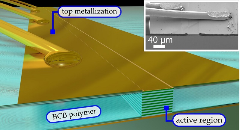
Illustration of an active element in the new integrated THz photonics platform, with the laser waveguide embedded in a low-loss benzocyclobutene (BCB) polymer and covered with an extended top metallization. The inset shows an electron microscope image of a fabricated device that features improved dispersion, RF, and thermal properties and can be co-integrated with various passive elements on the same photonic chip. Courtesy of U. Senica et al.
In the context of THz frequency combs, the researchers showed that control over transverse modes is essential to obtain a regular and flat-top comb spectrum, mainly with a reduction of the ridge lateral dimensions. For conventional double metal ridges, the width cannot be arbitrarily small since the waveguides are connected by wire bonding directly on the top metallic cladding. This inherently limits the effective ridge width to the dimensions of the bonding wire patch, making devices with ridges of 50 µm or below challenging to contact and prone to failure. Bonding directly on the active region can introduce defects, increasing the waveguide losses and nonintentionally selecting specific modes, potentially compromising the long-term performance of the device and its spectral characteristics.
The team’s planarized platform solved these issues. Placing the bonding wires on top of the extended top metallization over the passive, BCB-covered area prevented the formation of any defects or local hot spots on top of the active region. It enabled the fabrication of very narrow waveguides well below the bonding wire size.
The narrow waveguide width can be used as an efficient selection mechanism for the fundamental transversal lasing mode, and is also beneficial for heat dissipation and high-temperature continuous-wave operation. Moreover, the extended contact facilitates a lateral heat flow and eases the heat extraction as in a radiator scheme. This results in an improved measured maximum operating temperature of the planarized devices.
In addition to passive waveguides with low insertion loss, enabling the tuning of the laser cavity boundary conditions and the co-integration of active and passive elements on the same platform, the researchers said that with a strong external RF drive, they were able to produce actively mode-locked pulses as short as 4.4 ps.
The research was published in Light: Science & Applications (www.doi.org/10.1038/s41377-022-01058-2).