Modular integrated optics are finding both telecom and consumer electronics applications.
Dr. Hubert Kostal, NanoOpto Corp.
This year, integrated optics will begin to gain a significant foothold in commercial optical circuits, both in telecom and consumer electronics. Two years from now, they will most likely be predominant in optical circuits.
Such devices are built by fabricating optical nanostructures on optical wafers that are then diced to create compact, high-performance optical chips. The value of the integrated optics comes in reducing the size and cost and in increasing the functionality of an optical circuit. Multiple technologies — planar lightguide circuits, microelectromechanical systems (MEMS), liquid crystal, photonic crystals and nano-optics — are making strides toward providing these capabilities, but have yet to achieve critical mass in integrated optical circuit applications. The primary barriers to be overcome are threefold:
• Creating clear economic value in a meaningful application.
• Finding ways to integrate not just within a given technology, but also across technologies.
• Keeping manufacturing simple enough to realize high yields fast.
The tendency of proponents of integrated optics is often to emphasize monolithic integration of complex circuits. This is because the unique benefits of optical integration for size and promised cost are easier to promote when wiping the slate clean. The downside is that increased complexity in both manufacturing and implementing change can generate offsetting costs and result in delays in adoption of a new technology.

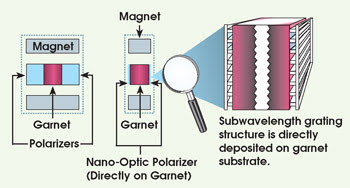
The ability to integrate manufacturing operations is likely to be the primary source of short-term success in optical integration at the wafer level, as illustrated by this simple optical isolator.
However, the key to realizing volume application of optical integration is more likely to involve a focus on relatively simple optical circuits and on creating value principally through manufacturing integration. Pragmatically, manufacturing integration should be considered at least as critical as functional integration, even though complete monolithic functional integration remains the longer-term goal.
With this in mind, we expect that key barriers to adoption of integrated optics will be overcome this year by looking broadly across the full spectrum of commercial applications of optical circuits for opportunities for integration. We also expect an emphasis on hybrid integration over monolithic integration, to provide incremental and readily realizable improvements for existing optical circuits. This will involve focusing on wafer-based manufacturing, borrowing efficiencies from semiconductor manufacturing.
Preliminary opportunities for optical integration that will be addressed successfully in 2004 are in consumer electronics (projection and other displays, cell phones, digital cameras and optical data storage), optical sensors and basic optical communications functions. These applications are characterized by the availability of simple, yet sophisticated, optical circuits embedded in commercial products. Optical integration will be introduced by combining as few as two discrete optical functions so that its principal value comes from the reduction of assembly costs and, only secondarily, of component costs.
Because near-term successful applications for optical integration will predominantly involve incremental enhancements of current optical circuits, hybrid integration — combining multiple optical technologies — is the most likely approach to generating commercial success this year. Finding ways to combine multiple materials and manufacturing processes supports more immediate optimization and cost reduction. Indeed, the capability for integrating manufacturing operations is likely to be the primary source of short-term success in optical integration.
The technologies that are the most promising contenders as the core for optical integration and near-term success — nano-optics, programmable logic controllers, photonic crystals and MEMS — all utilize wafer-based manufacturing processes, actively borrowing experience from semiconductor manufacturing to drive expenses down quickly in high-volume production. Near-term market penetration will require cost savings at lower production volumes or ramping up quickly for high-volume applications.
Within the next couple of years, end users can look for several trends in integrated optics. Companies will work to establish environmental and application reliability, to improve their manufacturing efficiencies to allow greater penetration at lower cost and to expand the optical circuit designer’s experience with the new capabilities. Concerted efforts will be made to improve the economics of customized integrated optics and to give new product architectures the time required to come to market, with the ultimate goal being predominantly monolithic optical circuit integration.
Meet the author
Hubert Kostal is vice president of marketing and sales at NanoOpto Corp. in Somerset, N.J.