3D Printing Focus of Nanoscribe US User Meeting
Nanoscribe GmbH, a 3D printer manufacturer, held its first U.S. user meeting — a two-day seminar — at Harvard University.

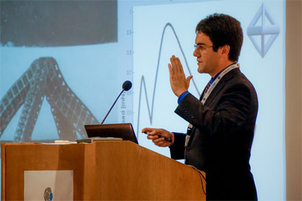
California Institute of Technology researcher Lucas Meza delivers a talk at Nanoscribe’s first U.S. user meeting. Courtesy of Nanoscribe GmbH.
In collaboration with the university’s Center for Nanoscale Systems (CNS), which houses a Nanoscribe laser lithography system, attendees were shown the latest software and hardware developments, along with areas of application for the Photonic Professional GT 3D printer. The technological possibilities range from the manufacture of extremely high-resolution mesoscale objects to applications in photonics and plasmonics, requiring structure sizes of just a few hundred nanometers.

Attendees at Nanoscribe’s first U.S. user meeting. Courtesy of Nanoscribe GmbH.
“The presentations by our clients on their various applications were the absolute highlight for me,” said Martin Hermatschweiler, CEO of Nanoscribe. “It is incredibly fascinating and enlightening to discover firsthand what different disciplinary fields are making use of our devices, which operate based on the principle of two-photon polymerization. The full scope of applications ranged from printing nanostructures at the CNS, to producing plasmonic displays at the University of Florida, to engineering new types of materials whose creation would have previously been impossible, as the scientists at Caltech presented.”
Nanoscribe develops compact tabletop laser lithography systems for 3D nanostructures.
/Buyers_Guide/Nanoscribe_GmbH_Co_KG/c18083