Infrared detectors are finding new applications and facing new challenges.
Hank Hogan, Contributing Editor
Where vision ends, infrared begins. Stretching from 0.7 to 1000 μm, the infrared spectrum covers a lot of ground, as do the imaging applications that make use of this part of the spectrum. These applications include biological studies, surveillance, fusion research and thermal imaging that highlights defects before a part fails. A look at various applications shows how infrared detectors are being used and what challenges for the technology remain.
Single nanotubes
The core market for Princeton Instruments/Acton of Trenton, N.J., is research imaging, which typically involves low-light situations. For investigators, IR wavelengths to 1.7 μm offer the chance to uncover new things. For example, infrared fluorescent reporters can be seen from deeper within a biological specimen than can visible fluorophores.
Some years ago, researchers at Rice University in Houston were interested in using carbon nanotubes ~1 nm in diameter as fluorophores. Biologically inert, the tubes can be attached to molecules. Importantly, they fluoresce in the near-IR.
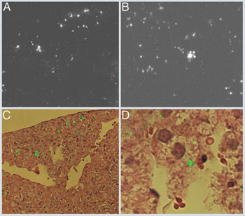
Figure 1. Single-wall nanotubes, carbon tubes 1 nm in diameter, fluoresce in the short-wave infrared (SWIR) from about 0.9 to 1.6 μm, so they can be used to probe biological tissues at greater depths than visible fluorophores. On top are infrared images captured with a Princeton Instruments/Acton InGaAs camera. These images are two magnifications of rabbit liver tissue 24 hours after intravenous administration of the nanotubes, with a field width of 390 μm on the left and 83 μm on the right. The larger features are from the nanotubes, while the isolated scattered bright pixels are sensor defects. In C and D, the nanotubes’ fluorescence from the images directly above is overlaid as false-color green onto visible bright-field images from adjacent 3-μm-thick specimen slices stained with hematoxylin and eosin. Reprinted with permission of PNAS.
Ravi Guntupalli, product marketing manager for imaging at Princeton Instruments, recalled that the researchers tried this first with a standard camera made for thermal imaging. They discovered the task to be at the limits of the system’s capabilities, largely because of the sensitivity needed to isolate a single nanotube. The investigators achieved results with a near-IR InGaAs-based imager from the company and are continuing the research (Figure 1).
An InGaAs-based solution was unavailable less than a decade ago because of manufacturing problems and materials issues. The most important issue for research applications was the dark current — the amount of electronic noise generated when no light strikes the sensor. It can be lowered by eliminating defects, which manufacturers have done over the past few years. However, decreasing dark current in infrared detectors is a struggle against nature. A longer-wavelength photon is less energetic than a shorter one; therefore, a semiconductor must have a narrower bandgap to detect it. However, a narrower bandgap increases the dark current. Guntupalli said that the company gets around the challenge by cooling with liquid nitrogen, but that having a lower starting dark current would be ideal.
Resolution and speed
Flir Systems Inc. of Wilsonville, Ore., makes imagers that span the infrared spectrum from the short-wave (SWIR, below 2 μm) to mid-wave (MWIR, up to 5 μm) and long-wave (LWIR, up to 13 μm). Its high-end products do not simply image an object; rather, they measure temperature point by point via thermography. This technique can be used for predictive maintenance because parts that are about to fail often show a thermal signature.
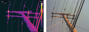
Figure 2. Thermal imagers operating in the long-wavelength infrared near 10 μm can reveal details not evident in the visible spectrum, and this information can be used for troubleshooting and predictive maintenance. This thermal image of a transformer-bearing telephone pole (left, with the visible on the right) is color-coded according to the scale on the right edge. In the upper left of the thermal image is a maximum temperature reading for the boxed area. Anomalous hot spots can indicate developing defects and so highlight where failure may occur. Courtesy of Flir.
Jerry Beeney, an engineer at the company noted that Flir has been working on increasing the resolution and frame rate of its products — parameters that lag behind what is possible with visible-wavelength cameras. With an eye toward improved resolution, the company announced in 2006 a handheld thermal camera with 640 x 480 pixels, four times larger than the 320 × 240 previously available. He said that achieving the comparatively small pixel counts was a materials issue, with the pixels in IR sensors being larger than those used in the visible. Those increased dimensions have a cascading effect.
“The pixel size for the infrared focal plane arrays is a little bit bigger than on a standard CCD. So the format grows fairly large as you start increasing the number of pixels,” he explained.
As for speed, last year the company debuted high-speed thermal cameras capable of 50 megapixels per second. The cameras can capture 640 × 512 pixels at 125 frames per second and can be used by the military in target signature analysis.
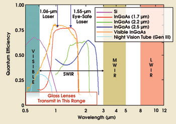
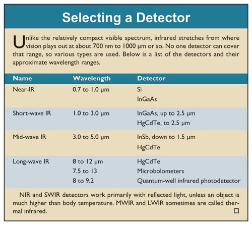
Figure 3. In the NIR/SWIR, silicon detectors fade out around 1 μm, while various incarnations of indium gallium arsenide are sensitive to wavelengths well past 2 μm. MWIR and LWIR have their own sensor materials and technologies. Courtesy of SUI, part of Goodrich Corp.
Beeney sees the trends for larger pixel arrays and faster cameras continuing. Prices should continue to fall, although the impact may be felt largely in lower-end cameras.
Doug Malchow is manager of commercial business development at Princeton, N.J.-based SUI, part of the Goodrich Corp. Speaking about the passive detection of people, he noted that his company’s products have strengths that complement other technologies. As a result, soldiers may identify an enemy sooner and more easily than would be possible without these auxiliary devices.
The company uses InGaAs semiconductor sensors that are sensitive from 0.9 to 1.7 μm (Figure 4). When the sun sets, things do not go completely dark for these cameras. “There is a night glow in the sky, a radiance that is in the 1.0- to 1.7-μm band emanating from the sky, and that illuminates objects that our camera can image,” Malchow said.
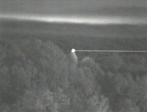
Figure 4. A 1.06-μm laser beam is clearly seen in this nighttime photo taken with an InGaAs sensor. The same sensors also can image a 1.55-μm light source, which is eye-safe and undetectable by conventional intensified visible sensors. Courtesy of SUI.
Because of their operating wavelength, the company’s cameras can see through smoke and clouds better than an intensified visible sensor can. An added bonus is that objects can be targeted and ranged with a light source at 1550 nm, invisible to the eye and to conventional night-vision sensors.
Although LWIR sensors can detect warm objects such as people and animals, Malchow noted that InGaAs offers something that long-wave detectors do not: resolution-derived clarity. Because of that, observers can tell a deer from a person, a vital bit of intelligence.
An SWIR camera combined with an LWIR detector would enable soldiers to spot an object and identify it. Such a combined sensor is a goal of the military. Another is to shrink pixel size and increase pixel count. At present, commercial devices are limited to 25-μm pixels because of the indium bumps used in the bonding process. As part of a military contract, the company has demonstrated a 20-μm pitch array and aims to produce a 15-μm-pitch megapixel InGaAs device sometime next year.
Princeton Scientific Instruments of Monmouth Junction, N.J., specializes in, among other things, very fast frame rate cameras. These have been available only in the visible, but the company is developing an extension of the technology that will work in infrared wavelengths from 1 to 4 μm and will capture data at up to a million frames per second. “It might be commercially available at the end of the year,” said company President John Lowrance.
The sensor achieves its speed because each pixel consists of a photosensitive element and an adjacent charge storage array. Every clock cycle, the charge from the photodetector is sent into the storage array, while older data is shifted down the array and the oldest data is dumped. At a trigger, the process is stopped and the desired image retrieved. That data can be from before or after the trigger, which can be vital when trying to capture a random event.
In building an infrared version, the company has had to change the photodetector, going with a Schottky-barrier infrared detector constructed by melting platinum and palladium into the silicon. The devices are being fabricated, and there is a chance that the development timetable may have to be changed if there are problems.
One application for a fast camera might be in fusion research. Fusion machines confine hot plasma within a magnetic bottle, but the process is not perfect. The plasma can brush against the vessel wall and deposit a considerable amount of energy there, thereby losing it. It is here that the high-speed camera comes in. “From these infrared images, one can calculate the wall temperature and, in turn, determine the rate that energy is being deposited — an important parameter,” Lowrance said.
At Jenoptik Laser, Optik, Systeme GmbH of Jena, Germany, a handheld camera based on an uncooled microbolometer sensor was recently introduced. In such a sensor, incoming thermal radiation strikes a grid of vanadium oxide sitting atop silicon and causes a change in temperature, which is converted to a change in electrical resistance. The camera is sensitive in the LWIR from 7.5 to 14 μm, with a better than 90-mK resolution (Figure 5).
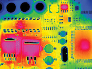
Figure 5. LWIR imagers that capture thermal radiation are used for printed circuit board inspection, seen here in a false-color image. Anomalous hot spots could indicate problems. The recent development of higher-resolution imagers allows the detection of smaller defects. Copyright by Jenoptik Laser, Optik, Systeme GmbH, Jena, Germany, 2006.
What makes this camera unusual is that it offers 640 × 480 pixels in a real-time mode but even more if proprietary optomechanical resolution technology is used.
“This is kind of a small scanning process, where you are able to record four times the resolution of the detector, which means, finally, 1.2-megapixel IR images,” said Heiko Richter, the company’s international sales manager for IR cameras.
The object cannot be moving so fast that the motion would be visible during the scan. However, for applications such as inspection of completed printed circuit boards for defects, the need to be essentially stationary is not a problem, and the higher resolution is a benefit.
Moreover, Richter said, microbolometers, as do other sensors, average temperature across a pixel. Thus, a subpixel hot or cold spot may not be readily found. A smaller pixel might allow previously unseen features to become detectable.
 Richter noted a trend toward a smaller pixel size because that factor drives the size of the detector, the associated optics and the final device. The military, a major purchaser, would like to minimize optic and camera size. Jenoptik’s new camera has a pixel pitch of 25 μm, with detector suppliers working to get that below 20 μm. However, an upper wavelength of 14 μm puts a lower limit on pixel size, which must remain bigger than the wavelength.
Making heat visible
Stuart Nixdorff, co-founder and vice president of sales and marketing at RedShift Systems Corp. in Burlington, Mass., has a magic number — $3000 — the threshold at which business tools become commonplace. It happened to PCs for office workers and to breathing apparatus for firefighters.
Nixdorff thinks that it will happen to thermal cameras as well, because an LWIR imager can penetrate the smoke that obscures a burning building and pinpoint hidden hot spots, something important to firefighters. “A very, very basic value proposition in fire service is that you go into a fire and you can’t see without a camera,” he said.
However, traditional thermal imaging technology is not cheap, with prices several times those of visible-wavelength digital cameras. RedShift proposes to surmount this problem by using what it calls a thermal light valve to make a standard CMOS imager see heat. The light valve absorbs incoming LWIR on one side, which changes the reflectance on the other side. That reflectance is probed by a laser at 800 nm, and the CMOS imager detects the change.
The pixelation in the valve is carried out by the thermal isolation of each location, something that the company accomplishes with a microelectromechanical systems manufacturing process. The pixel size of the product is 42 μm, the result of a trade-off between lens cost, performance and the manufacturing of the thermal light valve.
According to Nixdorff, the technology produces a camera with a very wide dynamic range, which is beneficial for firefighting because it is possible to clearly see a person standing next to a fire.
The company will sell its imaging module to original equipment manufacturers. It expects to deliver samples this summer, and commercial availability of the modules is planned for the fall.
As we went to press, RedShift also announced that it will work with Imagize LLC of Berkeley, Calif., to produce a fusion sensor combining visible and LWIR imaging. The companies contend that the combination will intelligently fuse thermal and visible imagery on a pixel-by-pixel basis. If successful, this could enable early and accurate detection, as well as full identification, of objects and intruders in darkness, fog, smoke, shadows and severe weather. Initial target applications include surveillance and asset protection in such areas as parking lots and campuses. No timetable as to product availability was announced.