With the modern AI workload intensifying, integrated photonics offers a promising solution with an eye toward the future of work.
YOSEF BEN-EZRA, NEWPHOTONICS
As the field of integrated photonics has transformed from one of theory into one of practice, rapid progress in materials
science, device design, and manufacturing processes in the past two decades has helped drive the commercialization of PICs for various applications. Today, photonic integration is characterized by multiple photonic components integrated onto a single chip. These highly efficient, compact, and
versatile devices represent a new frontier for advanced optical signal processing (OSP) and communications.

Artificial intelligence is prompting new and growing burdens on the data center infrastructure tasked with supporting massively computationally intensive workloads. Optical solutions, including those based on familiar components, are positioned to offer much-needed solutions. Courtesy of NewPhotonics.
Accordingly, the possibilities for these miniaturized photonic devices to transmit, manipulate, and process information have advanced beyond delivering data at
unprecedented speeds. Emerging PIC
innovations include heterogeneous integration of varying materials and technol-
ogies, ultrasecure compute quantum
photonics, neuromorphic photonics, and packaging. Each of these innovation
subfields exists outside the bounds of
ultrafast data and telecom, combining high levels of performance, reliability, and scale to deliver next-generation technology.
Advancements in these areas also carry the potential to extend beyond a core focus area of high technology today: the AI workload.
Yet, much of the current focus on
applying this transformative technology is tied to addressing existing bottlenecks and processes — as opposed to the
dynamic data management, processing,
and networking challenges that are forthcoming. Currently, the predominant goal is to use PICs to break down legacy processes and infrastructure barriers that are limiting on-pace growth of data-driven AI workloads and use cases. This high-level focus comes as AI revolutionizes industries at a global scale, placing an ever-growing burden on data center infrastructure to support computationally intensive workloads.
Meanwhile, the broader optical realm is charting a more immediate and sustainable path. In its aim to replace electrical dependence, its most obvious targets are the latency and power imperatives facing data connectivity for compute and transmission.
Photonic integration in the era of AI
Amid the present AI workflow, achieving low-latency inference with effective sub-millisecond response times is a primary concern. Real-time decision-making for AI-powered applications, as well as for autonomous vehicles and applications involving interactive user experiences, necessitates stringent infrastructure requirements. The complex computations and large data sets involved in AI inference can introduce significant latency, especially as models become more sophisticated. Strategies to address this latency challenge include using specialized hardware accelerators, implementing edge computing architectures that bring the processing closer to the data sources, and optimizing software and algorithms.
A parallel concern is energy consumption of AI workloads: The computational intensity of these applications leads to
significant power draw and cooling requirements. Data centers must simultaneously reduce energy usage and carbon footprint without compromising the
delivery of the processing power and
performance that AI workloads demand.
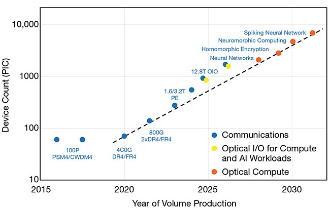
A forward-looking perspective and projection on scaling optics on silicon, with increased on-chip functionality via increased component integration for datacom pluggable modules.
Courtesy of NewPhotonics.
Data centers themselves also face increased challenges in physical space and resource use. Traditional server racks and computing infrastructure may not — and,
in fact, are unlikely to — accommodate the high-density computing requirements of modern AI applications. As data
centers seek ways to pack more AI processing power into limited physical spaces without sacrificing efficiency, cooling, or power distribution, they rely on density and efficiency of not only packaging but also technology innovation in the design and deployment of optical components.
PICs are a cornerstone of the ongoing data revolution. At the same time, emerging optical solutions and systems are poised to push boundaries even further to deliver advantages over both traditional electronics- and PICs-based systems. These performance gains will yield higher bandwidth, lower latency, and improved energy efficiency.
The PIC and beyond
The exponential growth of data-intensive applications spurred by the rise of cloud computing and cloud-based services, as well as big data, generative AI, and Internet of Things sensors, among other contributors, has stressed the limits of traditional electrical interconnects. These mechanisms rely on copper wiring and electronic switching and have struggled to keep pace with the insatiable demand for faster, more efficient data transmission. Combined with the physical limitations of miniaturization, these challenges have driven the search for alternative solutions that can overcome the inherent constraints that electrical systems commonly present.
Within this context of increasing
demand for higher performance, energy efficiency, and functionality, PICs and silicon photonics have more broadly
become viable alternatives. PICs have
delivered major improvements in size, cost, and performance compared to
discrete optical components.
In focusing on more than just the PIC element, the functionality of optical interconnects offers a promising solution to the limitations of electrical interconnects. Optical signals are immune to electromagnetic interference, allowing for higher-bandwidth and lower-latency
data transmission. Moreover, optical components are inherently more energy-efficient, because they do not suffer from the same heat generation and power consumption issues as their electronic counterparts. This makes them particu-
larly well suited for high-speed data transmission, real-time signal processing, and low-power applications.
Optical systems can also operate in harsh environments, making them ideal for industrial, defense, and space-based applications. Plus, integrating optical and electronic components on a single chip already enables the development of compact, multifunctional devices that can perform a wide range of sensing, imaging, computing, and communications tasks. From reconfigurable optical devices to heterogeneous integration and quantum optics, these advancements will enable high-speed, energy-efficient, and versatile optical systems that will be transformational across industry sectors.
The advantages to optical interconnects emerge as limitations to traditional PICs are increasingly apparent, particularly for use in telecom, data center, and sensing systems. Existing PICs face challenges in packaging and thermal management.
Further, the rigid, planar nature of traditional PIC architectures often limits the ability of a PIC to fully exploit the potential of nonlinear optical effects, such as for advanced functionalities in signal processing, sensing, and frequency conversion. And, integrating electronic and photonic components on a single chip has proved to be a significant technical hurdle. In many cases, it has lead to suboptimal performance and increased complexity.
Linear-drive pluggable optics
Linear-drive pluggable optics (LPO) represent an early and effective use of PICs to reduce power consumption and cost while meeting the demands of high-speed, high-density optical commun-
ication connections. Using a linear drive approach to replace power-hungry and
expensive digital signal processors (DSPs) with PICs demonstrates many of the efficiencies in PIC design to date; users are now using integrated photonics
capabilities to perform functions previously implemented via CMOS-based DSPs. In these deployments, the PIC(s) function(s) to drive the optical modulators
with enhancements, such as optical equalization.
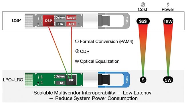
The implementation of optical pluggable transceivers in the all-optics paradigm promises to deliver improved performance as well as reduced power and latency. Such a solution also supports multivendor interoperability. CDR: clock and data recovery (circuit); LPO: linear-drive pluggable optics; LRO: linear receive optics; PD: photodiode; TIA: transimpedance amplifier. Courtesy of NewPhotonics.
The advantages of using LPO technology, especially in datacom and telecom, are considerable. LPO technology allows users to achieve low latency when replacing DSPs with PIC-based optical signal processors using linear modulators with channel equalization functionality. As a result, systems can achieve reduced power consumption by at least 50% compared to pluggable optical modules. An LPO approach can also significantly reduce overall materials costs. LPO-based designs support streamlined pluggable packaging, thereby simplifying any subsequent updates and/or scaling.
Critically, replacing DSPs with OSP mitigates link performance challenges and facilitates multivendor interoperability.
Yet, interoperability remains a limiting factor to the adoption of LPO. Due to the variation in channel characteristics, interoperability requires comparable signal processing capabilities. Still, this bottleneck has sparked some of the most significant contributions to OSP.
Meeting challenges
Remaining challenges must be addressed on several fronts to continue scaling true all-optical solutions. For one, integrating
optical components, such as lasers, modulators, and detectors, onto a single chip continues to present significant technical challenges. Scaling all-optical systems to support the growing demand for bandwidth and processing power also requires overcoming obstacles related to the efficient distribution and routing of optical signals as well as managing the interconnectivity between the optical
components that a system may use. Although optical components can be more energy-efficient than their electrical counterparts, the overall consumption of all optical systems, including the required supporting infrastructure, must be carefully managed to maintain the advantages of these technologies.
Reliability and stability pose additional challenges. Despite their operability in extreme environments, temperature
fluctuations and vibrations can limit
optical system performance. This is noticeable especially for mission-critical applications.
For these reasons, the widespread
adoption of all-optical interconnects
and systems will require a collaborative effort from stakeholders in the research and engineering communities as well
as industry. Continued progress to optical component technology, integration techniques, and system-level design will be crucial to bringing these transformative technologies further into the mainstream. It must also be coupled with the development of scalable, cost-effective manufacturing processes.
In the face of these challenges,
researchers and engineers pursuing
integrated photonics and other optical
solutions are exploring a range of
approaches. These range from the use of advanced materials — wide-bandgap semiconductors and 2D materials — to the development of 3D-integrated
photonic architectures, which use the third dimension to enhance device
density, improve optical routing, and
better exploit nonlinear optical phenomena. Additionally, integrating microelec-
tromechanical systems (MEMS) and reconfigurable optical elements has introduced new levels of tunability and adaptability to optical systems.
Combining advancements in these emerging technologies with advancements in photonic-electronic codesign and the latest packaging solutions indicates that the optical industry is poised to
unlock an era of high-performance, energy-efficient, and versatile integrated photonic systems. As the industry moves forward, and as innovations in signal
processing and networking become increasingly vital, a clear road map of technological progress, standardization efforts, and collaborative research will benefit all constituents.
The heart of PIC innovation
Integrated and silicon photonics have made significant contributions to the wider field of photonics and can be critically applied to the challenges ahead. Companies in the ecosystem are developing groundbreaking technologies such
as high-speed optical transceivers,
compact and energy-efficient photonic chips, and sophisticated sensing solutions.
By leveraging their agility and creativity, early commercial entities are often able
to bring these cutting-edge technologies to market faster than larger players who may also be more established in the marketplace.
At the same time, big industry is increasingly collaborative and eager to build on the agility and creativity of early innovators. This serves to push progress in a mutually beneficial ecosystem that is necessary to reach the full potential of all-optical integration. Meanwhile, others in the integrated photonics and silicon photonics space are applying rapid prototype, iterate, and novel technology approaches to this market, which is still in a phase of explosive development. Furthermore, companies are identifying still-unmet needs while simultaneously applying solution concepts that push the boundaries of what is possible.
Meet the author
Yosef Ben-Ezra is CTO at NewPhotonics and professor at Holon Institute of Technology
in Tel Aviv, Israel. His team develops innova-
tive photonics technology that aims to reduce the complexities of integrated photonic processing in data centers; email: [email protected].