Dr. Manoj Kanskar, Alfalight Inc.
The heart of a diode laser is the gain medium, known as the quantum well, which is buried inside a waveguide in the middle of a semiconductor junction. The quantum well has appropriately tailored energy levels such that an electric current through the diode produces a population inversion at the desired wavelength. The optical waveguide keeps the photons traveling in the proper direction, and a pair of mirrors completes the resonator.
Unfortunately, each of these elements introduces loss that reduces the laser’s power efficiency. These losses can occur optically (photons are scattered or absorbed) or electrically (electron-hole pairs fail to generate useful photons). An analysis of these phenomena yields five basic categories of loss:
• Below-threshold losses. A certain amount of the electrical input power is consumed simply to attain population inversion in the laser. Further, some of the electron-hole pairs created below threshold decay without producing photons.
• Band-alignment losses. The diode laser must overcome the voltage deficit resulting from misalignment of the band structure of the quantum well with various heterostructure interfaces. Until the deficit is overcome, useful optical power cannot be generated.
• Carrier leakage. Some electrons and holes do not make it into the quantum well to produce photons.
• Scattering and absorption. Some photons are scattered from imperfections in the semiconductor structure or from imperfect mirrors. Free carriers absorb additional photons.
• Joule heating. This results from the diode’s series resistance, which includes contact resistances as well as bulk resistance in the heterostructure itself, leading to I2R loss.
The expression for the maximum efficiency, ηp,max, is given by

where ηext is the external differential quantum efficiency (defined as the ratio of the number of laser photons produced by the laser to the number of electron-hole pairs injected), VF is the quasi-Fermi level difference, V0 is the overall built-in voltage, Rs is the series resistance, and Ith is the threshold current.1,2 From this, it is apparent that the four key means of improving ηp,max are maximizing ηext, and minimizing V0, Rs and Ith.
In CW operation, ηext is a function of temperature and is given by

where Th is the heat-sink temperature, ΔTj is the junction-temperature rise (i.e., T = Th + ΔTj), and T1 is the characteristic temperature coefficient for ηext that signifies how quickly the slope efficiency degrades with a rise in temperature. Because V0 is weakly dependent on temperature, the temperature dependence of hp,max is determined primarily by that of hp,max. Therefore, it is of paramount importance to improve the thermal properties of a diode laser by maximizing T1 and minimizing ΔTj.

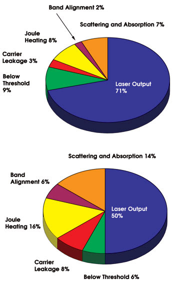
Figure 1. Improvements have boosted the electrical efficiency of a diode laser bar to 71 percent (top), obtained at a heat sink temperature of 25 °C. In a typical, 50-W, 970-nm diode laser bar (bottom), only 50 percent of the electrical input is converted to useful laser power.
As shown in the first equation, an increase in ηext and a reduction in V0 will have the most significant impact on maximizing the efficiency. We have realized dramatic improvements in efficiency by improving the internal injection efficiency through strain adjustments to the quantum-well barriers. This directly increases ηext by preventing the holes and electrons that are injected into the quantum well from leaking out of it. Additionally, we have reduced V0 by modifying the doping profile in the laser’s separate confinement heterostructure layer.
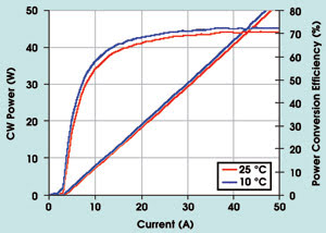
This preliminary optimization effort has resulted in electrical efficiencies of 71 and 73 percent at heat sink temperatures of 25 and 10 °C, respectively, at a wavelength of ~970 nm. All the loss mechanisms except below-threshold losses have been reduced in this laser (Figure 1). Moreover, the slope efficiency is greater than 1.1 W/A (Figure 2), which indicates a high external differential quantum efficiency. Further, the drive voltage is less than 1.5 V even at 50 A, reflecting the reduced built-in voltage of this heterostructure design.3,4

Figure 2. Electrical efficiencies of 71 and 73 percent were obtained at heat sink temperatures of 25 and 10 °C, respectively. The diode bar producing these results was 1 cm wide and had a 1-mm-long resonator.
Incremental changes to each of several design parameters will continue to improve the performance of these devices. We intend to reduce Joule heating by optimizing doping and minimizing contact resistance, voltage deficit by bandgap engineering of the hetero-interfaces, and scattering and absorption losses by judicious overlap of light field and dopants and by improved crystal quality. Through these improvements, we believe that the greater than 70 percent efficiencies already demonstrated in the laboratory can be achieved in production-quality bars within two years.
But the Defense Advanced Research Projects Agency’s goal is 80 percent efficiency, and to achieve this level in production bars, novel innovations probably will be necessary, particularly in reducing the below-threshold losses. A significant portion of these losses occurs because quantum wells confine holes and electrons in only one dimension. If the carriers could be confined in all three dimensions, the laser threshold would be reduced dramatically. Consequently, one of the methods that we are pursuing is the substitution of quantum dots for the quantum wells. The resulting delta-functionlike density of states would boost efficiency significantly.
As an alternate means of reducing threshold loss, we are growing quantum wells on unconventional (110)-oriented GaAs substrates. Quantum wells grown in this orientation have higher oscillator strengths, which increase intrinsic gain, and they thereby reduce the lasing threshold.
Both of these methods are challenging approaches to improving efficiency, but the potential payoff is significant and likely will be necessary to reach the goal of 80 percent electrical efficiency.
References
1. D. Botez et al (Oct. 10, 1996). 66% CW wallplug efficiency from Al-free 0.98 μm-emitting diode lasers. ELECTRONICS LETTERS, pp. 2012-2013.
2. D.P. Bour and A. Rosen (Oct. 1, 1989). Optimum cavity length for high conversion efficiency quantum well diode lasers. JOURNAL OF APPLIED PHYSICS, pp. 2813-2818.
3. M. Kanskar et al (2004). 17th Solid State and Diode Laser Technology Review Technical Digest.
4. M. Kanskar (Nov. 10, 2004). High Power Conversion Efficiency 970 nm Aluminum-Free Diode Lasers. LEOS 2004, session WC4.
Meet the author
Manoj Kanskar is vice president of research and development at Alfalight Inc. in Madison, Wis.; e-mail: [email protected].